- 您现在的位置:买卖IC网 > PDF目录268181 > NAND01GR3B3CZA1 (STMICROELECTRONICS) 128M X 8 FLASH 1.8V PROM, 35 ns, PBGA63 PDF资料下载
参数资料
| 型号: | NAND01GR3B3CZA1 |
| 厂商: | STMICROELECTRONICS |
| 元件分类: | PROM |
| 英文描述: | 128M X 8 FLASH 1.8V PROM, 35 ns, PBGA63 |
| 封装: | 9.50 X 12 MM, 1 MM HEIGHT, 0.80 MM PITCH, VFBGA-63 |
| 文件页数: | 20/59页 |
| 文件大小: | 998K |
| 代理商: | NAND01GR3B3CZA1 |
第1页第2页第3页第4页第5页第6页第7页第8页第9页第10页第11页第12页第13页第14页第15页第16页第17页第18页第19页当前第20页第21页第22页第23页第24页第25页第26页第27页第28页第29页第30页第31页第32页第33页第34页第35页第36页第37页第38页第39页第40页第41页第42页第43页第44页第45页第46页第47页第48页第49页第50页第51页第52页第53页第54页第55页第56页第57页第58页第59页
27/59
NAND512-B, NAND01G-B, NAND02G-B, NAND04G-B, NAND08G-B
Block Erase
Erase operations are done one block at a time. An
erase operation sets all of the bits in the ad-
dressed block to ‘1’. All previous data in the block
is lost.
An erase operation consists of three steps (refer to
1.
One bus cycle is required to setup the Block
Erase command. Only addresses A18-A27
(x8) or A17-A26 (x16) are used, the other
address inputs are ignored.
2.
two or three bus cycles are then required to
load the address of the block to be erased.
addresses of each device.
3.
one bus cycle is required to issue the Block
Erase confirm command to start the P/E/R
Controller.
The operation is initiated on the rising edge of
write Enable, W, after the confirm command is is-
sued. The P/E/R Controller handles Block Erase
and implements the verify process.
During the Block Erase operation, only the Read
Status Register and Reset commands will be ac-
cepted, all other commands will be ignored.
Once the program operation has completed the P/
E/R Controller bit SR6 is set to ‘1’ and the Ready/
Busy signal goes High. If the operation completed
successfully, the Write Status Bit SR0 is ‘0’, other-
wise it is set to ‘1’.
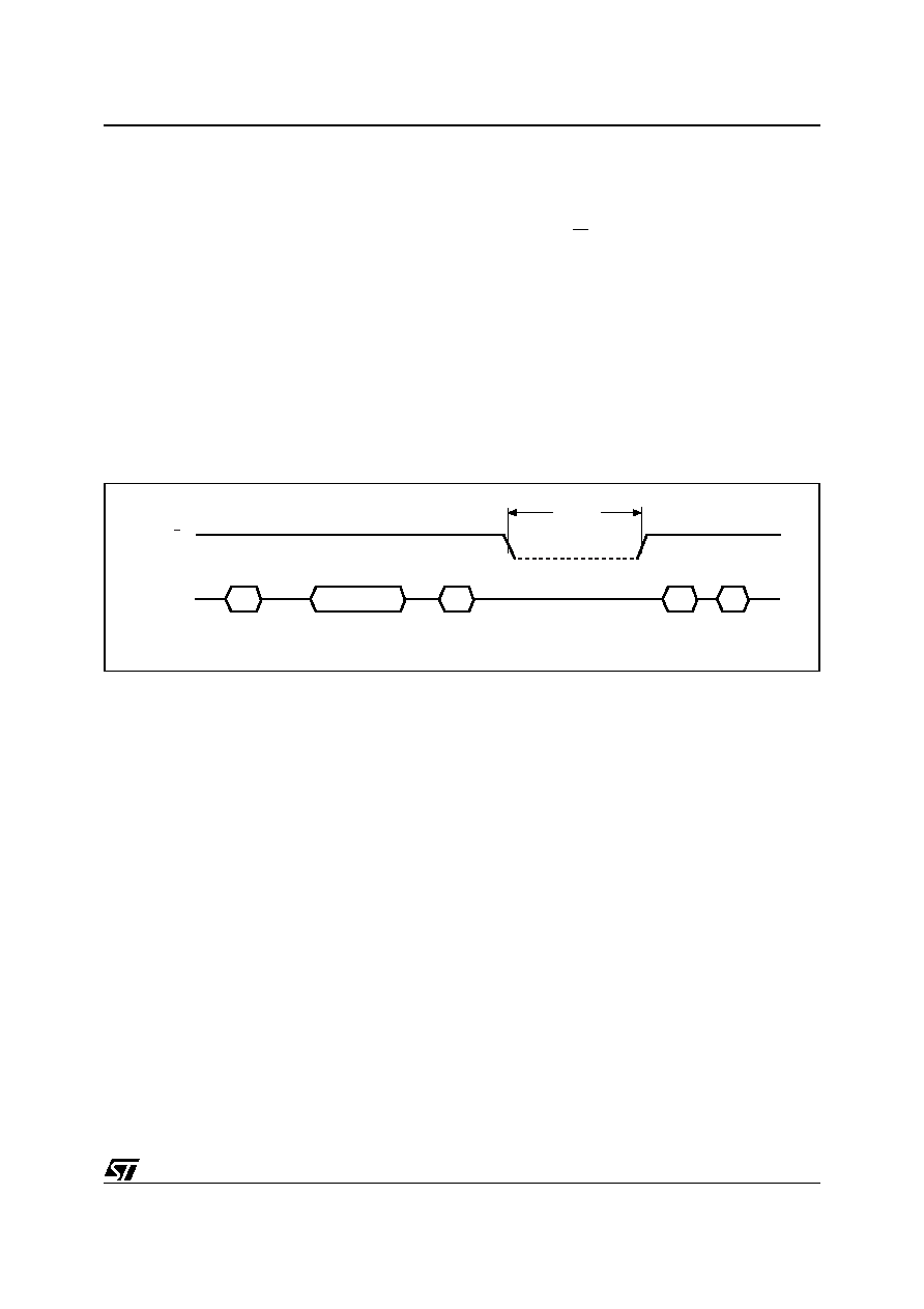
Figure 17. Block Erase Operation
Reset
The Reset command is used to reset the Com-
mand Interface and Status Register. If the Reset
command is issued during any operation, the op-
eration will be aborted. If it was a program or erase
operation that was aborted, the contents of the
memory locations being modified will no longer be
valid as the data will be partially programmed or
erased.
If the device has already been reset then the new
Reset command will not be accepted.
The Ready/Busy signal goes Low for tBLBH4 after
the Reset command is issued. The value of tBLBH4
depends on the operation that the device was per-
forming when the command was issued, refer to
Table 25. for the values.
I/O
RB
Block Address
Inputs
SR0
ai07593
D0h
70h
60h
Block Erase
Setup Code
Confirm
Code
Read Status Register
Busy
tBLBH3
(Erase Busy time)
相关PDF资料 |
PDF描述 |
|---|---|
| NAND02GR4B2BZB1 | 128M X 16 FLASH 1.8V PROM, 35 ns, PBGA63 |
| NCH030A3-FREQ-OUT27 | CRYSTAL OSCILLATOR, CLOCK, 1 MHz - 4 MHz, HCMOS OUTPUT |
| NTHA3JAA3-FREQ-OUT27 | CRYSTAL OSCILLATOR, CLOCK, 1 MHz - 4 MHz, HCMOS OUTPUT |
| NTHA3KC3-FREQ-OUT27 | CRYSTAL OSCILLATOR, CLOCK, 1 MHz - 4 MHz, HCMOS OUTPUT |
| NCHA80C3-FREQ1-OUT27 | CRYSTAL OSCILLATOR, CLOCK, 24 MHz - 80 MHz, HCMOS OUTPUT |
相关代理商/技术参数 |
参数描述 |
|---|---|
| NAND01GR3M0AZB5E | 制造商:STMICROELECTRONICS 制造商全称:STMicroelectronics 功能描述:256/512Mb/1Gb (x8/x16, 1.8/3V, 528 Byte Page) NAND Flash Memories + 256/512Mb (x16/x32, 1.8V) LPSDRAM, MCP |
| NAND01GR3M0AZB5F | 制造商:STMICROELECTRONICS 制造商全称:STMicroelectronics 功能描述:256/512Mb/1Gb (x8/x16, 1.8/3V, 528 Byte Page) NAND Flash Memories + 256/512Mb (x16/x32, 1.8V) LPSDRAM, MCP |
| NAND01GR3M0AZC5E | 制造商:STMICROELECTRONICS 制造商全称:STMicroelectronics 功能描述:256/512Mb/1Gb (x8/x16, 1.8/3V, 528 Byte Page) NAND Flash Memories + 256/512Mb (x16/x32, 1.8V) LPSDRAM, MCP |
| NAND01GR3M0AZC5F | 制造商:STMICROELECTRONICS 制造商全称:STMicroelectronics 功能描述:256/512Mb/1Gb (x8/x16, 1.8/3V, 528 Byte Page) NAND Flash Memories + 256/512Mb (x16/x32, 1.8V) LPSDRAM, MCP |
| NAND01GR3M0BZB5E | 制造商:STMICROELECTRONICS 制造商全称:STMicroelectronics 功能描述:256/512Mb/1Gb (x8/x16, 1.8/3V, 528 Byte Page) NAND Flash Memories + 256/512Mb (x16/x32, 1.8V) LPSDRAM, MCP |
发布紧急采购,3分钟左右您将得到回复。