参数资料
| 型号: | NCP5332ADWR2 |
| 厂商: | ON Semiconductor |
| 文件页数: | 12/30页 |
| 文件大小: | 0K |
| 描述: | IC CTRLR BUCK 2PH STEPDWN 28SOIC |
| 产品变化通告: | Product Obsolescence 11/Feb/2009 |
| 标准包装: | 1 |
| 应用: | 控制器,高性能处理器 |
| 输入电压: | 4.5 V ~ 14 V |
| 输出数: | 2 |
| 输出电压: | 可调 |
| 工作温度: | 0°C ~ 70°C |
| 安装类型: | 表面贴装 |
| 封装/外壳: | 28-SOIC(0.295",7.50mm 宽) |
| 供应商设备封装: | 28-SOIC |
| 包装: | 剪切带 (CT) |
| 其它名称: | NCP5332ADWR2OSCT |
第1页第2页第3页第4页第5页第6页第7页第8页第9页第10页第11页当前第12页第13页第14页第15页第16页第17页第18页第19页第20页第21页第22页第23页第24页第25页第26页第27页第28页第29页第30页
�� �
�
�NCP5332A�
�APPLICATIONS� INFORMATION�
�Overview�
�The� NCP5332A� DC/DC� controller� from� ON�
�Semiconductor� was� developed� using� the� Enhanced� V� 2�
�topology� to� meet� requirements� of� low� voltage,� high� current�
�loads� with� fast� transient� requirements.� Enhanced� V� 2� combines�
�the� original� V� 2� topology� with� peak� current?mode� control� for�
�fast� transient� response� and� current� sensing� capability.� The�
�addition� of� an� internal� PWM� ramp� and� implementation� of�
�fast?feedback� directly� from� V� CORE� has� improved� transient�
�response� and� simplified� design.� The� NCP5332A� includes�
�Power� Good� (PWRGD)� and� MOSFET� gate� drivers� to�
�provide� a� “fully� integrated� solution”� to� simplify� design,�
�minimize� circuit� board� area,� and� reduce� overall� system� cost.�
�Two� advantages� of� a� multi?phase� converter� over� a�
�single?phase� converter� are� current� sharing� and� increased�
�apparent� output� frequency.� Current� sharing� allows� the�
�designer� to� use� less� inductance� in� each� phase� than� would� be�
�required� in� a� single?phase� converter.� The� smaller� inductor�
�will� produce� larger� ripple� currents� but� the� total� per� phase�
�power� dissipation� is� reduced� because� the� RMS� current� is� lower.�
�Transient� response� is� improved� because� the� control� loop� will�
�measure� and� adjust� the� current� faster� in� a� smaller� output�
�inductor.� Increased� apparent� output� frequency� is� desirable�
�because� the� off� time� and� the� ripple� voltage� of� the� two?phase�
�converter� will� be� less� than� that� of� a� single?phase� converter.�
�Fixed� Frequency� Multi?Phase� Control�
�In� a� multi?phase� converter,� multiple� converters� are�
�connected� in� parallel� and� are� switched� on� at� different� times.�
�This� reduces� output� current� from� the� individual� converters�
�and� increases� the� apparent� ripple� frequency.� Because� several�
�converters� are� connected� in� parallel,� output� current� can� ramp�
�up� or� down� faster� than� a� single� converter� (with� the� same�
�value� output� inductor)� and� heat� is� spread� among� multiple�
�components.�
�The� NCP5332A� controller� uses� two?phase,� fixed�
�frequency,� Enhanced� V� 2� architecture� to� measure� and� control�
�n� =� 1� or� 2�
�currents� in� individual� phases.� Each� phase� is� delayed� 180� °�
�from� the� previous� phase.� Normally,� GATE(H)� transitions� to�
�a� high� voltage� at� the� beginning� of� each� oscillator� cycle.�
�Inductor� current� ramps� up� until� the� combination� of� the�
�current� sense� signal,� the� internal� ramp� and� the� output� voltage�
�ripple� trip� the� PWM� comparator� and� bring� GATE(H)� low.�
�Once� GATE(H)� goes� low,� it� will� remain� low� until� the�
�beginning� of� the� next� oscillator� cycle.� While� GATE(H)� is�
�high,� the� Enhanced� V� 2� loop� will� respond� to� line� and� load�
�variations.� On� the� other� hand,� once� GATE(H)� is� low,� the� loop�
�can� not� respond� until� the� beginning� of� the� next� PWM� cycle.�
�Therefore,� constant� frequency� Enhanced� V� 2� will� typically�
�respond� to� disturbances� within� the� off?time� of� the� converter.�
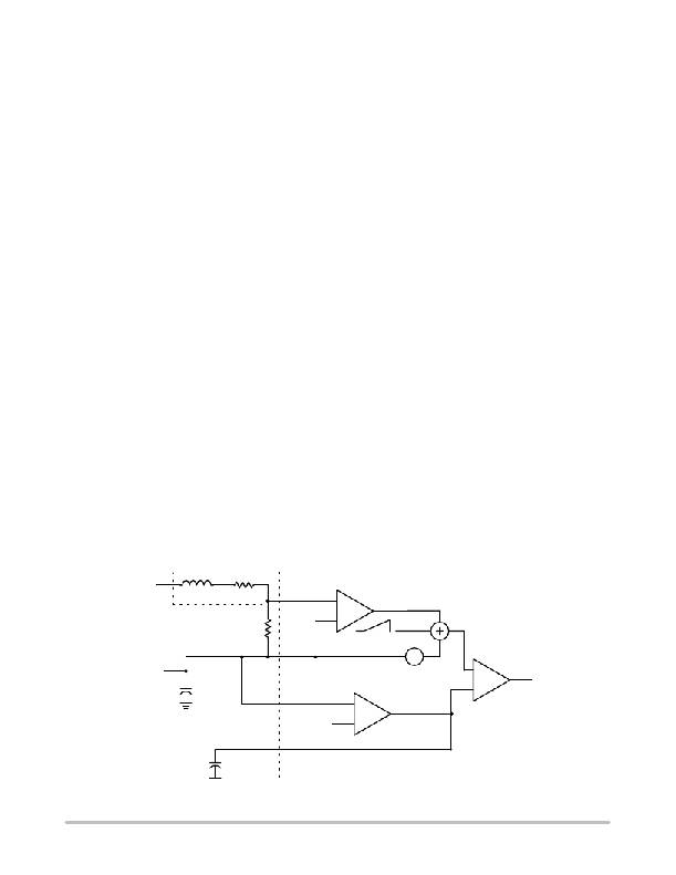
�The� Enhanced� V� 2� architecture� measures� and� adjusts� the�
�output� current� in� each� phase.� An� additional� input� (CSn)� for�
�inductor� current� information� has� been� added� to� the� V� 2� loop�
�for� each� phase� as� shown� in� Figure� 10.� The� triangular� inductor�
�current� is� measured� differentially� across� RS,� amplified� by�
�CSA� and� summed� with� the� Channel� Startup� Offset,� the�
�Internal� Ramp,� and� the� Output� Voltage� at� the� non?inverting�
�input� of� the� PWM� comparator.� The� purpose� of� the� Internal�
�Ramp� is� to� compensate� for� propagation� delays� in� the�
�NCP5332A.� This� provides� greater� design� flexibility� by�
�allowing� smaller� external� ramps,� lower� minimum� pulse�
�widths,� higher� frequency� operation,� and� PWM� duty� cycles�
�above� 50%� without� external� slope� compensation.� As� the�
�sum� of� the� inductor� current� and� the� internal� ramp� increase,�
�the� voltage� on� the� positive� pin� of� the� PWM� comparator� rises�
�and� terminates� the� PWM� cycle.� If� the� inductor� starts� a� cycle�
�with� higher� current,� the� PWM� cycle� will� terminate� earlier�
�providing� negative� feedback.� The� NCP5332A� provides� a�
�CSn� input� for� each� phase,� but� the� CS� REF� and� COMP� inputs�
�are� common� to� all� phases.� Current� sharing� is� accomplished�
�by� referencing� all� phases� to� the� same� CS� REF� and� COMP�
�pins,� so� that� a� phase� with� a� larger� current� signal� will� turn� off�
�earlier� than� a� phase� with� a� smaller� current� signal.�
�SWNODE�
�Ln�
�RLn�
�CSn�
�+�
�CSA�
�COn�
�RSn�
�Internal� Ramp�
�V� OUT�
�(V� CORE� )�
�+�
�CS� REF�
�“Fast?Feedback”�
�Connection�
�?+�
�Channel�
�Start?Up�
�+�
�To� F/F�
�Reset�
�V� FB�
�DAC�
�Out�
�E.A.�
�+�
�Offset�
�PWM�
�COMP�
�COMP�
�+�
�Figure� 10.� Enhanced� V� 2� Control� Employing� Resistive� Current� Sensing� and� Additional� Internal� Ramp�
�http://onsemi.com�
�12�
�相关PDF资料 |
PDF描述 |
|---|---|
| X4283PI-2.7A | IC SUPERVISOR CPU 128K EE 8-DIP |
| GMC26DRYI-S13 | CONN EDGECARD 52POS .100 EXTEND |
| X4323V8-2.7 | IC SUPERVISOR CPU 32K EE 8-TSSOP |
| HMM24DRYH-S13 | CONN EDGECARD 48POS .156 EXTEND |
| NCP5331FTR2 | IC CTRLR BUCK 2PH PWM DRV 32LQFP |
相关代理商/技术参数 |
参数描述 |
|---|---|
| NCP5338MNR2G | 制造商:ON Semiconductor 功能描述:INTEGRATED DRIVER AND MOS - Tape and Reel 制造商:ON Semiconductor 功能描述:INTEGRATED DRIVER AND MOS - Cut TR (SOS) 制造商:ON Semiconductor 功能描述:REEL / INTEGRATED DRIVER AND MOS 制造商:ON Semiconductor 功能描述:Integrated Driver and MOSFET |
| NCP5351 | 制造商:ONSEMI 制造商全称:ON Semiconductor 功能描述:4 A Synchronous Buck Power MOSFET Driver |
| NCP5351/D | 制造商:未知厂家 制造商全称:未知厂家 功能描述:4A Synchronous Buck Power Mosfet Driver |
| NCP5351D | 功能描述:功率驱动器IC 5V 4A Dual MOSFET RoHS:否 制造商:Micrel 产品:MOSFET Gate Drivers 类型:Low Cost High or Low Side MOSFET Driver 上升时间: 下降时间: 电源电压-最大:30 V 电源电压-最小:2.75 V 电源电流: 最大功率耗散: 最大工作温度:+ 85 C 安装风格:SMD/SMT 封装 / 箱体:SOIC-8 封装:Tube |
| NCP5351DG | 功能描述:功率驱动器IC 5V 4A Dual MOSFET RoHS:否 制造商:Micrel 产品:MOSFET Gate Drivers 类型:Low Cost High or Low Side MOSFET Driver 上升时间: 下降时间: 电源电压-最大:30 V 电源电压-最小:2.75 V 电源电流: 最大功率耗散: 最大工作温度:+ 85 C 安装风格:SMD/SMT 封装 / 箱体:SOIC-8 封装:Tube |
发布紧急采购,3分钟左右您将得到回复。