- 您现在的位置:买卖IC网 > PDF目录189259 > NT56V6620C0T-75 (NANYA TECHNOLOGY CORP) SYNCHRONOUS DRAM, PDSO54 PDF资料下载
参数资料
| 型号: | NT56V6620C0T-75 |
| 厂商: | NANYA TECHNOLOGY CORP |
| 元件分类: | DRAM |
| 英文描述: | SYNCHRONOUS DRAM, PDSO54 |
| 封装: | 0.400 INCH, SSOP2-54 |
| 文件页数: | 18/66页 |
| 文件大小: | 1701K |
| 代理商: | NT56V6620C0T-75 |
第1页第2页第3页第4页第5页第6页第7页第8页第9页第10页第11页第12页第13页第14页第15页第16页第17页当前第18页第19页第20页第21页第22页第23页第24页第25页第26页第27页第28页第29页第30页第31页第32页第33页第34页第35页第36页第37页第38页第39页第40页第41页第42页第43页第44页第45页第46页第47页第48页第49页第50页第51页第52页第53页第54页第55页第56页第57页第58页第59页第60页第61页第62页第63页第64页第65页第66页
NT56V6610C0T NT56V6620C0T
64Mb : x8 x16
PC133 / PC100 Synchronous DRAM
REV 1.1 June, 2000
25
NANYA TECHNOLOGY CORP.
NANYA TECHNOLOGY CORP. reserves the right to change Products and Specifications without notice.
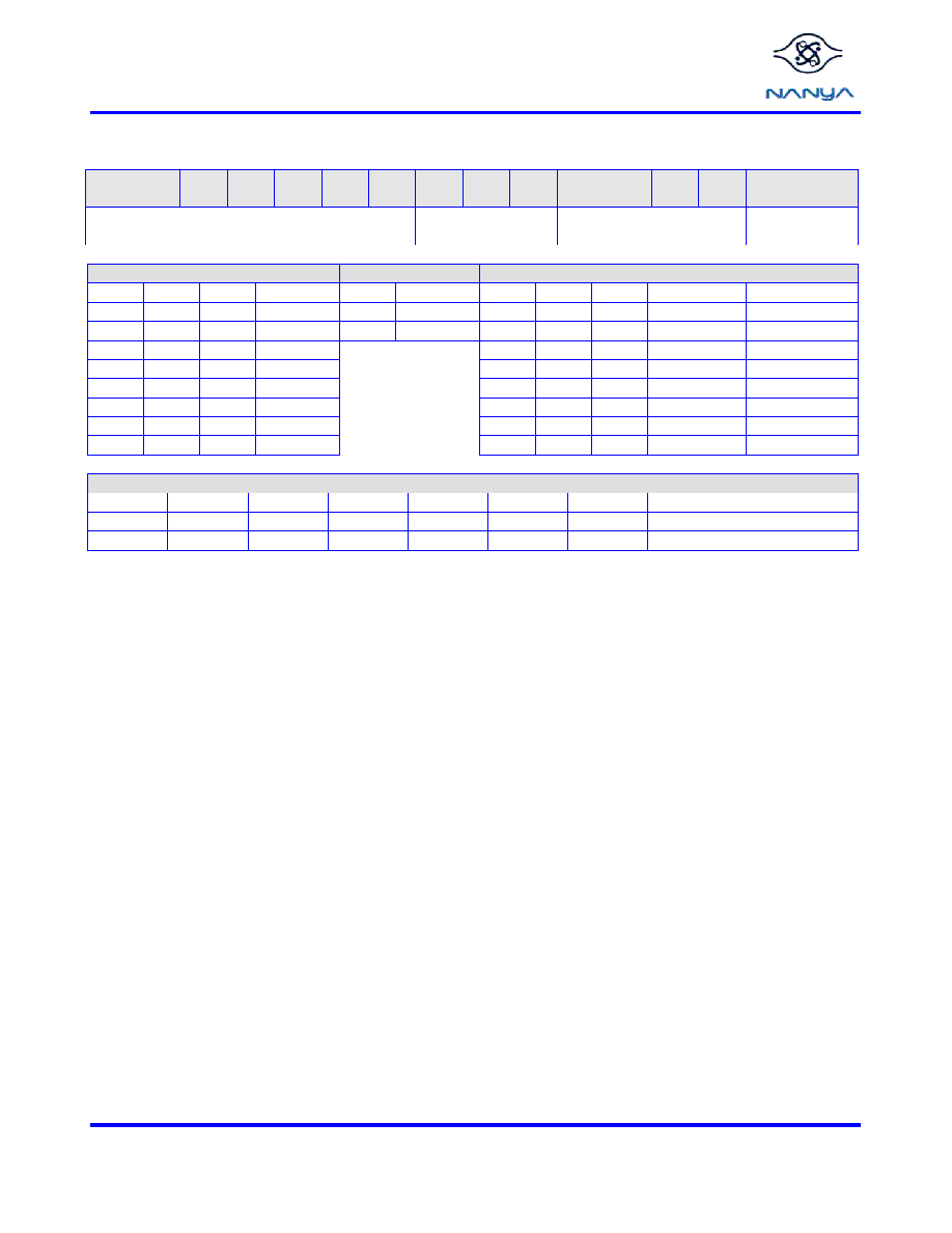
Mode Register Definition
Mode Register set: (Programming mode)
A13
A12
A11
A10
A9
A8
A7
A6
A5
A4
A3
A2
A1
A0
Address bus
(Ax)
Operation Mode
CAS Latency
BT
Burst Length
Mode Register
(Mx)
CAS Latency
Burst Type
Burst Length
M6
M5
M4
Latency
M3
Type
M2
M1
M0
BT=0
BT=1
0
Reserved
0
Sequential
0
1
0
1
Reserved
1
Interleave
0
1
2
0
1
0
2
0
1
0
4
0
1
3
0
1
8
1
0
Reserved
1
0
Reserved
1
0
1
Reserved
1
0
1
Reserved
1
0
Reserved
1
0
Reserved
1
Reserved
1
Full Page
Reserved
Operation Mode
M13
M12
M11
M10
M9
M8
M7
Mode
0
Normal
0
1
0
Multiple Burst with Single Write
Burst Mode Operation
Burst mode operation is used to provide a constant flow of data to memory locations (write cycle), or from memory locations (read cycle).
Three parameters define how the burst mode will operate: burst sequence, burst length, and operation mode. The burst sequence and burst
length are programmable and are determined by address bits A0 - A3 during the Mode Register Set command. Operation mode is also
programmable and is set by address bits A7 - A13.
Burst sequence defines the order in which the burst data will be delivered or stored to the SDRAM. The two types of burst sequence
supported are sequential and interleaved. See the table below.
The burst length controls the number of bits that will be output after a Read Command, or the number of bits to be input after a Write
Command. The burst length can be programmed to have values of 1, 2, 4, 8 or full page (actual page length is dependent on organization:
x4, x8, or x16). Full page burst operation is only possible using the sequential burst type.
Burst operation mode can be normal operation or multiple burst with single write operation. Normal operation implies that the device will
perform burst operations on both read and write cycles until the desired burst length is satisfied. Multiple burst with single write operation
was added to support Write Through Cache operation. Here, the programmed burst length only applies to read cycles. All write cycles are
single write operations when this mode is selected.
相关PDF资料 |
PDF描述 |
|---|---|
| NT5CB256M4AN-BF | DDR DRAM, PBGA78 |
| NT5DS64M8BF-6KI | DDR DRAM, PBGA60 |
| NT5SE8M16DS-6K | 8M X 16 SYNCHRONOUS DRAM, 5 ns, PDSO54 |
| NT5SV8M8DT-7 | 8M X 8 SYNCHRONOUS DRAM, 5.4 ns, PDSO54 |
| NTC1111-20MHZ | Analog IC |
相关代理商/技术参数 |
参数描述 |
|---|---|
| NT5CB128M16FP-DI | 制造商:Nanya Technology Corporation 功能描述: 制造商:Nanya Technology Corporation 功能描述:MEMORY IC |
| NT5CB128M16FP-DIA | 制造商:Nanya Technology Corporation 功能描述:MEMORY IC |
| NT5CB128M16FP-DII | 制造商:Nanya Technology Corporation 功能描述:MEMORY IC |
| NT5CB128M16HP-CG | 制造商:Nanya Technology Corporation 功能描述:DRAM |
| NT5CB128M8FN-DH | 制造商:Nanya Technology Corporation 功能描述:MEMORY IC |
发布紧急采购,3分钟左右您将得到回复。