- 您现在的位置:买卖IC网 > PDF目录189259 > NT56V6620C0T-75 (NANYA TECHNOLOGY CORP) SYNCHRONOUS DRAM, PDSO54 PDF资料下载
参数资料
| 型号: | NT56V6620C0T-75 |
| 厂商: | NANYA TECHNOLOGY CORP |
| 元件分类: | DRAM |
| 英文描述: | SYNCHRONOUS DRAM, PDSO54 |
| 封装: | 0.400 INCH, SSOP2-54 |
| 文件页数: | 5/66页 |
| 文件大小: | 1701K |
| 代理商: | NT56V6620C0T-75 |
第1页第2页第3页第4页当前第5页第6页第7页第8页第9页第10页第11页第12页第13页第14页第15页第16页第17页第18页第19页第20页第21页第22页第23页第24页第25页第26页第27页第28页第29页第30页第31页第32页第33页第34页第35页第36页第37页第38页第39页第40页第41页第42页第43页第44页第45页第46页第47页第48页第49页第50页第51页第52页第53页第54页第55页第56页第57页第58页第59页第60页第61页第62页第63页第64页第65页第66页
NT56V6610C0T NT56V6620C0T
64Mb : x8 x16
PC133 / PC100 Synchronous DRAM
REV 1.1 June, 2000
13
NANYA TECHNOLOGY CORP.
NANYA TECHNOLOGY CORP. reserves the right to change Products and Specifications without notice.
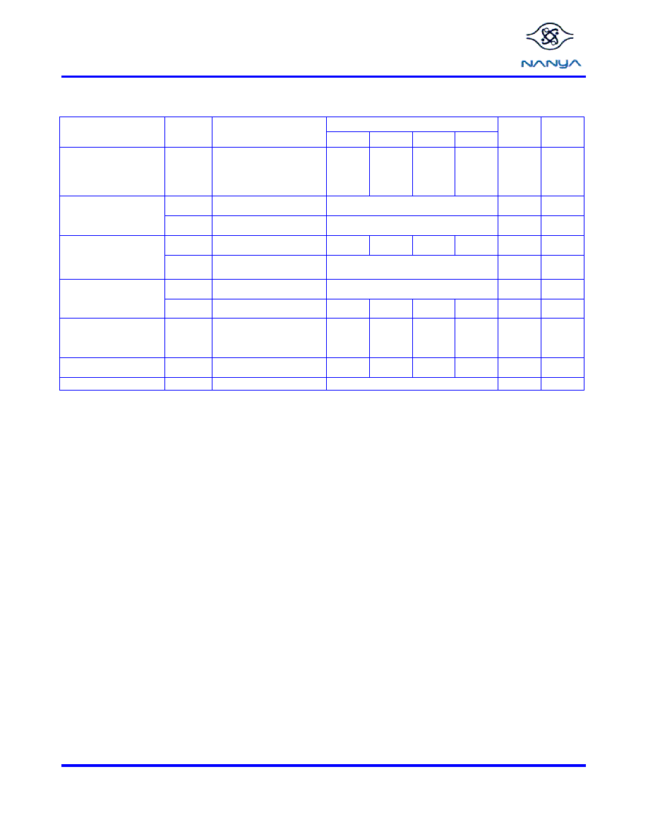
Operating, Standby, and Refresh Currents (VDD =3.3V ± 10% , T
A =0°C to 70°C)
Version
Parameter
Symbol
Test condition
- 7
- 75(B)
- 8B
- 8A
Unit
Note
Operating current
ICC1
1 bank operation ,
tRC = tRC(mim), tCK = min
Active-Precharge
Command cycling
without burst operation
75
70
mA
1,2,3
ICC2P
CKE <= VIL(max),
tCK = min, /CS = VIH(min),
2
mA
1
Precharge
standby current
in power-down mode
ICC2PS
CKE <= VIL(max), tCK =oo,
/CS = VIH(min)
2
mA
1
ICC2N
CKE >= VIH(min),
/CS = VIH(min), tCK = min
35
25
mA
1
Precharge
standby current in non
power-down mode
ICC2NS
CKE >= VIH(min), tCK =oo
5
mA
1,5
ICC3P
CKE<=VIL(max), tCK =min
3
mA
1,7
No Operating current
( Active state : 4 bank)
ICC3N
CKE >=VIH(min),
/CS = VIH(min), tCK =min
40
30
mA
1,5
Operating current
( Burst mode )
ICC4
t CK =min , Read/ Write
command cycling,
Multiple banks active,
gapless data, BL=4
120
90
mA
1,6
Auto(CBR)
refresh current
ICC5
t RC = tRC(min) ; tCK =min
CBR command cycling
145
140
mA
1,3,4
Self refresh current
ICC6
CKE <= 0.2V
1
mA
1
Note :
1. Currents given are valid for a single device. The total current for a stacked device depends on the operation being performed on the
other deck.
2. These parameters depend on the cycle rate and are measured with the cycle determined by the minimum value of
t and t .Input signals are changed up to three times during t (min).
3. The specified values are obtained with the output open.
4. Input signals are changed once during t (min).
5. Input signals are changed once during three clock cycles.
6. Active Standby Current will be higher if Clock Suspend is entered during a burst read cycle (add 1mA per DQ).
7. Input signals are stable.
相关PDF资料 |
PDF描述 |
|---|---|
| NT5CB256M4AN-BF | DDR DRAM, PBGA78 |
| NT5DS64M8BF-6KI | DDR DRAM, PBGA60 |
| NT5SE8M16DS-6K | 8M X 16 SYNCHRONOUS DRAM, 5 ns, PDSO54 |
| NT5SV8M8DT-7 | 8M X 8 SYNCHRONOUS DRAM, 5.4 ns, PDSO54 |
| NTC1111-20MHZ | Analog IC |
相关代理商/技术参数 |
参数描述 |
|---|---|
| NT5CB128M16FP-DI | 制造商:Nanya Technology Corporation 功能描述: 制造商:Nanya Technology Corporation 功能描述:MEMORY IC |
| NT5CB128M16FP-DIA | 制造商:Nanya Technology Corporation 功能描述:MEMORY IC |
| NT5CB128M16FP-DII | 制造商:Nanya Technology Corporation 功能描述:MEMORY IC |
| NT5CB128M16HP-CG | 制造商:Nanya Technology Corporation 功能描述:DRAM |
| NT5CB128M8FN-DH | 制造商:Nanya Technology Corporation 功能描述:MEMORY IC |
发布紧急采购,3分钟左右您将得到回复。