- 您现在的位置:买卖IC网 > PDF目录189259 > NT56V6620C0T-75 (NANYA TECHNOLOGY CORP) SYNCHRONOUS DRAM, PDSO54 PDF资料下载
参数资料
| 型号: | NT56V6620C0T-75 |
| 厂商: | NANYA TECHNOLOGY CORP |
| 元件分类: | DRAM |
| 英文描述: | SYNCHRONOUS DRAM, PDSO54 |
| 封装: | 0.400 INCH, SSOP2-54 |
| 文件页数: | 8/66页 |
| 文件大小: | 1701K |
| 代理商: | NT56V6620C0T-75 |
第1页第2页第3页第4页第5页第6页第7页当前第8页第9页第10页第11页第12页第13页第14页第15页第16页第17页第18页第19页第20页第21页第22页第23页第24页第25页第26页第27页第28页第29页第30页第31页第32页第33页第34页第35页第36页第37页第38页第39页第40页第41页第42页第43页第44页第45页第46页第47页第48页第49页第50页第51页第52页第53页第54页第55页第56页第57页第58页第59页第60页第61页第62页第63页第64页第65页第66页
NT56V6610C0T NT56V6620C0T
64Mb : x8 x16
PC133 / PC100 Synchronous DRAM
REV 1.1 June, 2000
16
NANYA TECHNOLOGY CORP.
NANYA TECHNOLOGY CORP. reserves the right to change Products and Specifications without notice.
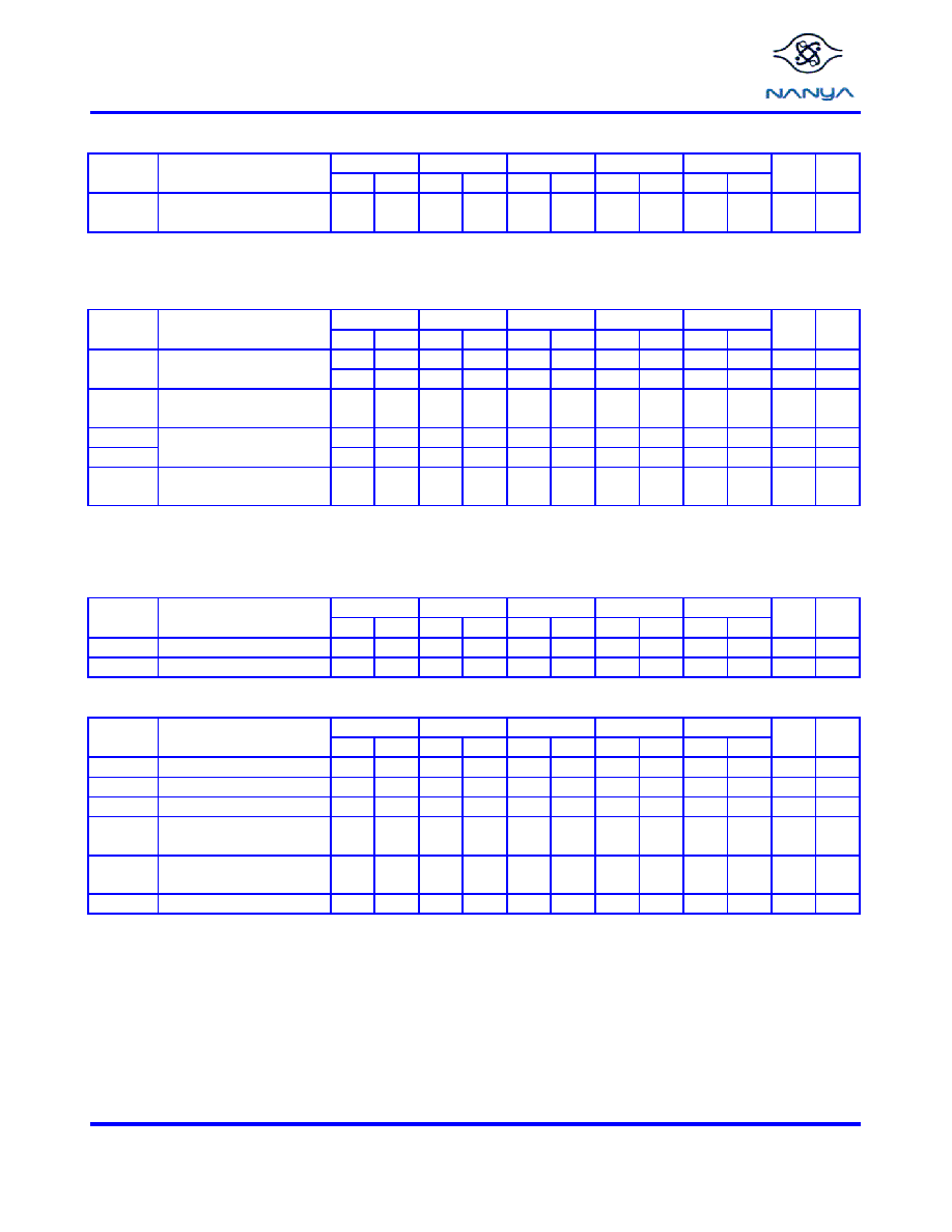
Mode Register Set Cycle
- 7
- 75B
- 75
- 8B
- 8A
Symbol
Parameter
Min.
Max.
Min.
Max.
Min.
Max.
Min.
Max.
Min.
Max.
Unit
Note
tRSC
Mode Register Set
Cycle Time
2
-
2
-
2
-
2
-
2
-
CLK
1
1.These parameters account for the number of clock cycle and depend on the operating frequency of the clock, as follows: the number of
clock cycles = specified value of timing / clock period (count fractions as a whole number).
Read Cycle
- 7
- 75B
- 75
- 8B
- 8A
Symbol
Parameter
Min.
Max.
Min.
Max.
Min.
Max.
Min.
Max.
Min.
Max.
Unit
Note
2.5
-
2.5
-
2.5
-
ns
1
tOH
Data Out Hold Time
2.7
-
2.7
-
3
-
3
-
ns
2
tLZ
Data Out to Low Impedance
Time
0
-
0
-
0
-
0
-
0
-
ns
tHZ3
3
6
3
5.4
3
5.4
3
6
3
6
ns
3
tHZ2
Data Out to High
Impedance Time
-
3
6
3
8
ns
3
tDQZ
DQM Data Out Disable
Latency
2
-
2
-
2
-
2
-
2
-
CLK
1.AC Output Load Circuit A.
2.AC Output Load Circuit B.
3.Referenced to the time at which the output achieves the open circuit condition, not to output voltage levels.
Refresh Cycle
- 7
- 75B
- 75
- 8B
- 8A
Symbol
Parameter
Min.
Max.
Min.
Max.
Min.
Max.
Min.
Max.
Min.
Max.
Unit
Note
tREF
Refresh Period
-
64
-
64
-
64
-
64
-
64
ms
tSREX
Self Refresh Exit Time
10
-
10
-
10
-
10
-
10
-
ns
Write Cycle
- 7
- 75B
- 75
- 8B
- 8A
Symbol
Parameter
Min.
Max.
Min.
Max.
Min.
Max.
Min.
Max.
Min.
Max.
Unit
Note
tDS
Data In Set-up Time
2
-
1.5
-
1.5
-
2
-
2
-
ns
tDH
Data In Hold Time
1
-
0.8
-
0.8
-
1
-
1
-
ns
tDPL
Data input to Precharge
14
-
15
-
15
-
15
-
15
-
ns
tDAL3
Data In to Active Delay
/CAS Latency = 3
5
-
5
-
5
-
5
-
5
-
CLK
tDAL2
Data In to Active Delay
/CAS Latency = 2
-
4
-
3
-
CLK
tDQW
DQM Write Mask Latency
0
-
0
-
0
-
0
-
0
-
ns
相关PDF资料 |
PDF描述 |
|---|---|
| NT5CB256M4AN-BF | DDR DRAM, PBGA78 |
| NT5DS64M8BF-6KI | DDR DRAM, PBGA60 |
| NT5SE8M16DS-6K | 8M X 16 SYNCHRONOUS DRAM, 5 ns, PDSO54 |
| NT5SV8M8DT-7 | 8M X 8 SYNCHRONOUS DRAM, 5.4 ns, PDSO54 |
| NTC1111-20MHZ | Analog IC |
相关代理商/技术参数 |
参数描述 |
|---|---|
| NT5CB128M16FP-DI | 制造商:Nanya Technology Corporation 功能描述: 制造商:Nanya Technology Corporation 功能描述:MEMORY IC |
| NT5CB128M16FP-DIA | 制造商:Nanya Technology Corporation 功能描述:MEMORY IC |
| NT5CB128M16FP-DII | 制造商:Nanya Technology Corporation 功能描述:MEMORY IC |
| NT5CB128M16HP-CG | 制造商:Nanya Technology Corporation 功能描述:DRAM |
| NT5CB128M8FN-DH | 制造商:Nanya Technology Corporation 功能描述:MEMORY IC |
发布紧急采购,3分钟左右您将得到回复。