- 您现在的位置:买卖IC网 > PDF目录224604 > NT5SV8M16FT-75BI (NANYA TECHNOLOGY CORP) 8M X 16 SYNCHRONOUS DRAM, 5.4 ns, PDSO54 PDF资料下载
参数资料
| 型号: | NT5SV8M16FT-75BI |
| 厂商: | NANYA TECHNOLOGY CORP |
| 元件分类: | DRAM |
| 英文描述: | 8M X 16 SYNCHRONOUS DRAM, 5.4 ns, PDSO54 |
| 封装: | 0.400 MM, PLASTIC, TSSOP2-54 |
| 文件页数: | 22/65页 |
| 文件大小: | 739K |
| 代理商: | NT5SV8M16FT-75BI |
第1页第2页第3页第4页第5页第6页第7页第8页第9页第10页第11页第12页第13页第14页第15页第16页第17页第18页第19页第20页第21页当前第22页第23页第24页第25页第26页第27页第28页第29页第30页第31页第32页第33页第34页第35页第36页第37页第38页第39页第40页第41页第42页第43页第44页第45页第46页第47页第48页第49页第50页第51页第52页第53页第54页第55页第56页第57页第58页第59页第60页第61页第62页第63页第64页第65页
NT5SV8M16FS / NT5SV8M16FT
128Mb Synchronous DRAM
REV 1.4
08/2009
29
NANYA TECHNOLOGY CORPORATION
NANYA reserves the right to change products and specifications without notice.
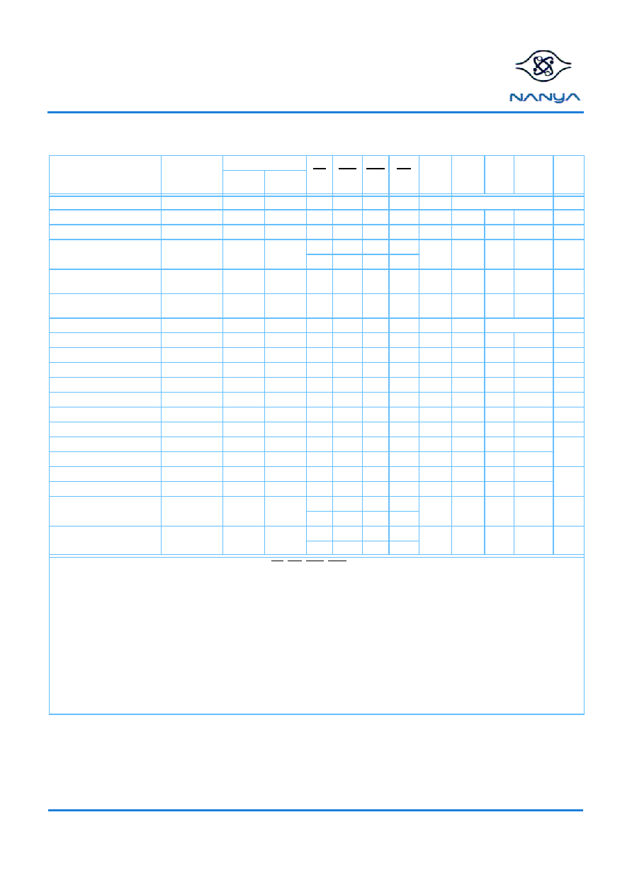
Command Truth Table (See note 1)
Function
Device State
CKE
CS
RAS
CAS
WE
DQM
BA0,
BA1
A10
A11,
A9-A0
Notes
Previous
Cycle
Current
Cycle
Mode Register Set
Idle
H
X
L
X
OP Code
Auto (CBR) Refresh
Idle
H
L
H
X
Entry Self Refresh
Idle
H
L
H
X
Exit Self Refresh
Idle (Self-
Refresh)
L
H
X
L
H
Single Bank Precharge
See Current
State Table
H
X
L
H
L
X
BS
L
X
2
Precharge all Banks
See Current
State Table
H
X
L
H
L
X
H
X
Bank Activate
Idle
H
X
L
H
X
BS
Row Address
2
Write
Active
H
X
L
H
L
X
BS
L
Column
2
Write with Auto-Precharge
Active
H
X
L
H
L
X
BS
H
Column
2
Read
Active
H
X
L
H
L
H
X
BS
L
Column
2
Read with Auto-Precharge
Active
H
X
L
H
L
H
X
BS
H
Column
2
Reserved
H
X
L
H
L
X
No Operation
Any
H
X
L
H
X
Device Deselect
Any
H
X
H
X
Clock Suspend Mode Entry
Active
H
L
X
4
Clock Suspend Mode Exit
Active
L
H
X
Data Write/Output Enable
Active
H
X
L
X
5
Data Mask/Output Disable
Active
H
X
H
X
Power Down Mode Entry
Idle/Active
H
L
H
X
6, 7
L
H
Power Down Mode Exit
Any (Power
Down)
L
H
X
6, 7
L
H
1. All of the SDRAM operations are defined by states of CS, WE, RAS, CAS, and DQM at the positive rising edge of the clock. Refer to the
Current State Truth Table.
2. Bank Select (BA0, BA1): BA0, BA1 = 0,0 selects bank 0; BA0, BA1 = 1,0 selects bank 1; BA0, BA1 = 0,1 selects bank 2; BA0, BA1 = 1,1
selects bank 3.
3. Not applicable.
4. During normal access mode, CKE is held high and CK is enabled. When it is low, it freezes the internal clock and extends data Read and
Write operations. One clock delay is required for mode entry and exit.
5. The DQM has two functions for the data DQ Read and Write operations. During a Read cycle, when DQM goes high at a clock timing the
data outputs are disabled and become high impedance after a two-clock delay. DQM also provides a data mask function for Write cycles.
When it activates, the Write operation at the clock is prohibited (zero clock latency).
6. All banks must be precharged before entering the Power Down Mode. (If this command is issued during a burst operation, the device
state will be Clock Suspend Mode.) The Power Down Mode does not perform any refresh operations; therefore the device can’t remain in
this mode longer than the Refresh period (tREF) of the device. One clock delay is required for mode entry and exit.
7. A No Operation or Device Deselect Command is required on the next clock edge following CKE going high.
相关PDF资料 |
PDF描述 |
|---|---|
| NT5TU64M16DG-3C | 64M X 16 DDR DRAM, 0.45 ns, PBGA84 |
| NTA2425E | |
| NTA2425F | |
| NTA2410-10 | |
| NTD2410F | |
相关代理商/技术参数 |
参数描述 |
|---|---|
| NT5SV8M16HS-6K | 制造商:Nanya Technology Corporation 功能描述:DRAM |
| NT5SV8M8DT | 制造商:未知厂家 制造商全称:未知厂家 功能描述:64Mb Synchronous DRAM |
| NT5SV8M8DT-6K | 制造商:未知厂家 制造商全称:未知厂家 功能描述:64Mb Synchronous DRAM |
| NT5SV8M8DT-7 | 制造商:未知厂家 制造商全称:未知厂家 功能描述:64Mb Synchronous DRAM |
| NT5SV8M8DT-7K | 制造商:未知厂家 制造商全称:未知厂家 功能描述:64Mb Synchronous DRAM |
发布紧急采购,3分钟左右您将得到回复。