- 您现在的位置:买卖IC网 > Datasheet目录488 > NTF6P02T3G (ON Semiconductor)MOSFET PWR P-CHAN 10A 20V SOT223 Datasheet资料下载
参数资料
| 型号: | NTF6P02T3G |
| 厂商: | ON Semiconductor |
| 文件页数: | 1/6页 |
| 文件大小: | 0K |
| 描述: | MOSFET PWR P-CHAN 10A 20V SOT223 |
| 产品变化通告: | Reactivation Notice 08/Apr/2011 Product Obsolescence 14/Apr/2010 |
| 标准包装: | 1 |
| FET 型: | MOSFET P 通道,金属氧化物 |
| FET 特点: | 逻辑电平门 |
| 漏极至源极电压(Vdss): | 20V |
| 电流 - 连续漏极(Id) @ 25° C: | 10A |
| 开态Rds(最大)@ Id, Vgs @ 25° C: | 50 毫欧 @ 6A,4.5V |
| Id 时的 Vgs(th)(最大): | 1V @ 250µA |
| 闸电荷(Qg) @ Vgs: | 20nC @ 4.5V |
| 输入电容 (Ciss) @ Vds: | 1200pF @ 16V |
| 功率 - 最大: | 8.3W |
| 安装类型: | 表面贴装 |
| 封装/外壳: | TO-261-4,TO-261AA |
| 供应商设备封装: | SOT-223 |
| 包装: | 剪切带 (CT) |
| 其它名称: | NTF6P02T3GOSCT |
��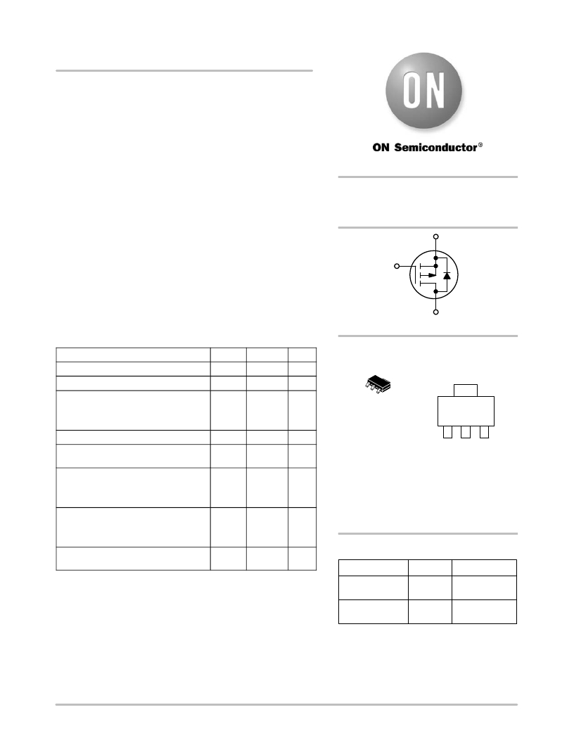 �
�
�NTF6P02,� NVF6P02�
�Power� MOSFET�
�-10� Amps,� -20� Volts�
�P� ?� Channel� SOT� ?� 223�
�Features�
�?� Low� R� DS(on)�
�?� Logic� Level� Gate� Drive�
�?� Diode� Exhibits� High� Speed,� Soft� Recovery�
�?� Avalanche� Energy� Specified�
�?� NVF� Prefix� for� Automotive� and� Other� Applications� Requiring�
�Unique� Site� and� Control� Change� Requirements;� AEC� ?� Q101�
�http://onsemi.com�
�?� 10� AMPERES�
�?� 20� VOLTS�
�R� DS(on)� =� 44� m� W� (Typ.)�
�S�
�?�
�Qualified� and� PPAP� Capable*�
�These� Devices� are� Pb� ?� Free� and� are� RoHS� Compliant�
�G�
�Typical� Applications�
�?� Power� Management� in� Portables� and� Battery� ?� Powered� Products,�
�i.e.:� Cellular� and� Cordless� Telephones� and� PCMCIA� Cards�
�D�
�P� ?� Channel� MOSFET�
�MAXIMUM� RATINGS� (T� J� =� 25� °� C� unless� otherwise� noted)�
�Rating� Symbol� Value�
�Unit�
�MARKING� DIAGRAM�
�&� PIN� ASSIGNMENT�
�3�
�Drain� ?� to� ?� Source� Voltage�
�Gate� ?� to� ?� Source� Voltage�
�Drain� Current� (Note� 1)�
�?� Continuous� @� T� A� =� 25� °� C�
�?� Continuous� @� T� A� =� 70� °� C�
�?� Single� Pulse� (t� p� =� 10� m� s)�
�Total� Power� Dissipation� @� T� A� =� 25� °� C�
�Operating� and� Storage� Temperature� Range�
�V� DSS�
�V� GS�
�I� D�
�I� D�
�I� DM�
�P� D�
�T� J� ,� T� stg�
�?� 20�
�±� 8.0�
�?� 10�
�?� 8.4�
�?� 35�
�8.3�
�?� 55� to�
�+150�
�Vdc�
�Vdc�
�Adc�
�Apk�
�W�
�°� C�
�4�
�1�
�2�
�SOT� ?� 223�
�CASE� 318E�
�STYLE� 3�
�1�
�Gate�
�Drain�
�4�
�AYW�
�6P02� G�
�G�
�2� 3�
�Drain� Source�
�Single� Pulse� Drain� ?� to� ?� Source� Avalanche� E� AS� 150� mJ�
�Energy� ?� Starting� T� J� =� 25� °� C�
�(V� DD� =� ?� 20� Vdc,� V� GS� =� ?� 5.0� Vdc,�
�I� L(pk)� =� ?� 10� A,� L� =� 3.0� mH,� R� G� =� 25� W� )�
�Thermal� Resistance� °� C/W�
�?� Junction� to� Lead� (Note� 1)� R� q� JL� 15�
�?� Junction� to� Ambient� (Note� 2)� R� q� JA� 71.4�
�?� Junction� to� Ambient� (Note� 3)� R� q� JA� 160�
�Maximum� Lead� Temperature� for� Soldering� T� L� 260� °� C�
�Purposes,� 1/8� ″� from� case� for� 10� seconds�
�Stresses� exceeding� Maximum� Ratings� may� damage� the� device.� Maximum�
�Ratings� are� stress� ratings� only.� Functional� operation� above� the� Recommended�
�Operating� Conditions� is� not� implied.� Extended� exposure� to� stresses� above� the�
�Recommended� Operating� Conditions� may� affect� device� reliability.�
�1.� Steady� State.�
�2.� When� surface� mounted� to� an� FR4� board� using� 1”� pad� size,�
�(Cu.� Area� 1.127� sq� in),� Steady� State.�
�3.� When� surface� mounted� to� an� FR4� board� using� minimum� recommended� pad�
�size,� (Cu.� Area� 0.412� sq� in),� Steady� State.�
�A� =� Assembly� Location�
�Y� =� Year�
�W� =� Work� Week�
�6P02� =� Specific� Device� Code�
�G� =� Pb� ?� Free� Package�
�(Note:� Microdot� may� be� in� either� location)�
�ORDERING� INFORMATION�
�Device� Package� Shipping� ?�
�NTF6P02T3G� SOT� ?� 223� 4000� /� Tape� &�
�(Pb� ?� Free)� Reel�
�NVF6P02T3G*� SOT� ?� 223� 4000� /� Tape� &�
�(Pb� ?� Free)� Reel�
�?For� information� on� tape� and� reel� specifications,�
�including� part� orientation� and� tape� sizes,� please�
�refer� to� our� Tape� and� Reel� Packaging� Specifications�
�Brochure,� BRD8011/D.�
�?� Semiconductor� Components� Industries,� LLC,� 2013�
�August,� 2013� ?� Rev.� 6�
�1�
�Publication� Order� Number:�
�NTF6P02T3/D�
�相关PDF资料 |
PDF描述 |
|---|---|
| NTGD3133PT1G | MOSFET P-CH DUAL 20V 21.5A 6TSOP |
| NTGD3147FT1G | MOSFET P-CH 20V 2.2A 6-TSOP |
| NTGD3148NT1G | MOSFET N-CH DUAL 20V 3.5A 6TSOP |
| NTGD3149CT1G | MOSFET COMPL 20V DUAL 6-TSOP |
| NTGD4161PT1G | MOSFET P-CH DUAL 30V 2.3A 6-TSOP |
相关代理商/技术参数 |
参数描述 |
|---|---|
| NT-FA-1-3/4-0 | 制造商:TE Connectivity 功能描述: |
| NTFKCN321 | 制造商:Omron Corporation 功能描述: |
| NTFR1/2 | 制造商: 功能描述: 制造商:undefined 功能描述: |
| NTFR-1/2-0-350MM | 制造商:TE Connectivity 功能描述:NTFR-1/2-0-350MM |
| NTFR-1/2-0-ASP | 制造商:TE Connectivity 功能描述:NEOPRENE ELASTOMER TUBING |
发布紧急采购,3分钟左右您将得到回复。