- 您现在的位置:买卖IC网 > Datasheet目录490 > NTMD2C02R2SG (ON Semiconductor)MOSFET N/P-CH COMPL 20V 8-SOIC Datasheet资料下载
参数资料
| 型号: | NTMD2C02R2SG |
| 厂商: | ON Semiconductor |
| 文件页数: | 11/12页 |
| 文件大小: | 0K |
| 描述: | MOSFET N/P-CH COMPL 20V 8-SOIC |
| 产品变化通告: | Wire Change 20/Aug/2008 Product Discontinuation 01/Oct/2008 |
| 标准包装: | 2,500 |
| FET 型: | N 和 P 沟道 |
| FET 特点: | 逻辑电平门 |
| 漏极至源极电压(Vdss): | 20V |
| 电流 - 连续漏极(Id) @ 25° C: | 5.2A,3.4A |
| 开态Rds(最大)@ Id, Vgs @ 25° C: | 43 毫欧 @ 4A,4.5V |
| Id 时的 Vgs(th)(最大): | 1.2V @ 250µA |
| 闸电荷(Qg) @ Vgs: | 20nC @ 4.5V |
| 输入电容 (Ciss) @ Vds: | 1100pF @ 10V |
| 功率 - 最大: | 2W |
| 安装类型: | 表面贴装 |
| 封装/外壳: | 8-SOIC(0.154",3.90mm 宽) |
| 供应商设备封装: | 8-SOICN |
| 包装: | 带卷 (TR) |
�� �
�
�NTMD2C02R2�
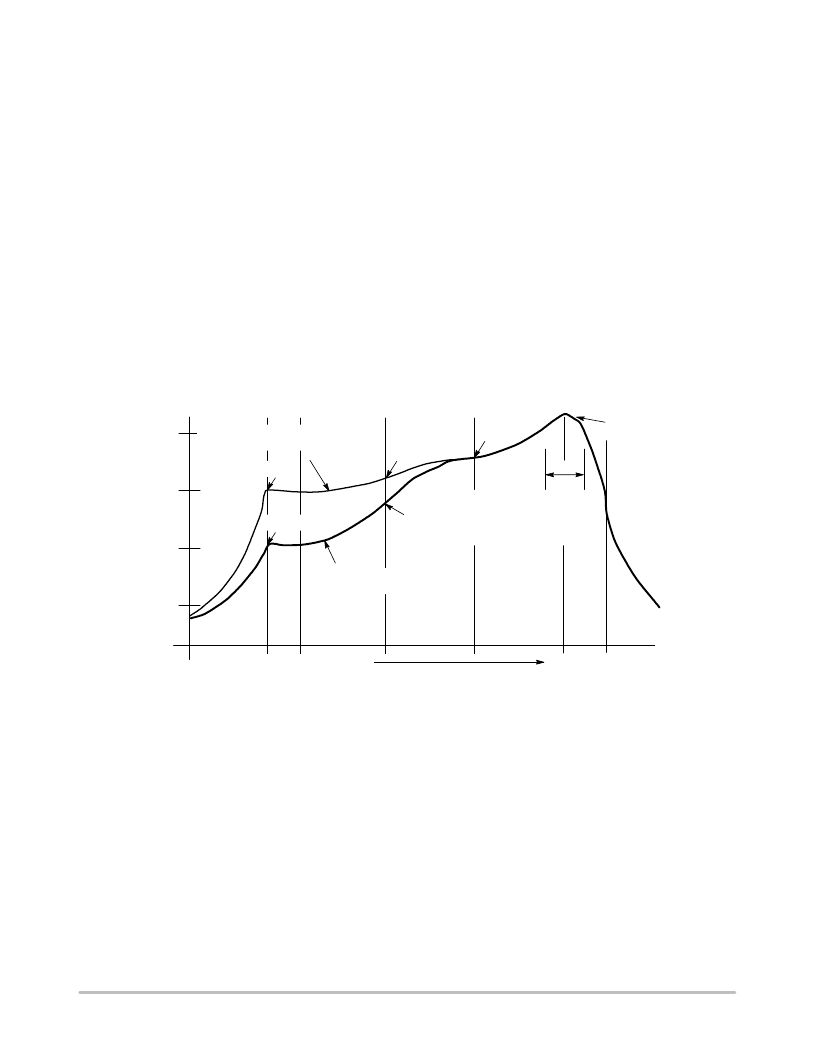
�TYPICAL� SOLDER� HEATING� PROFILE�
�For� any� given� circuit� board,� there� will� be� a� group� of�
�control� settings� that� will� give� the� desired� heat� pattern.� The�
�operator� must� set� temperatures� for� several� heating� zones�
�and� a� figure� for� belt� speed.� Taken� together,� these� control�
�settings� make� up� a� heating� “profile”� for� that� particular�
�circuit� board.� On� machines� controlled� by� a� computer,� the�
�computer� remembers� these� profiles� from� one� operating�
�session� to� the� next.� Figure� 26� shows� a� typical� heating�
�profile� for� use� when� soldering� a� surface� mount� device� to� a�
�printed� circuit� board.� This� profile� will� vary� among�
�soldering� systems,� but� it� is� a� good� starting� point.� Factors�
�that� can� affect� the� profile� include� the� type� of� soldering�
�system� in� use,� density� and� types� of� components� on� the�
�board,� type� of� solder� used,� and� the� type� of� board� or�
�substrate� material� being� used.� This� profile� shows�
�temperature� versus� time.� The� line� on� the� graph� shows� the�
�actual� temperature� that� might� be� experienced� on� the� surface�
�of� a� test� board� at� or� near� a� central� solder� joint.� The� two�
�profiles� are� based� on� a� high� density� and� a� low� density�
�board.� The� Vitronics� SMD310� convection/infrared� reflow�
�soldering� system� was� used� to� generate� this� profile.� The� type�
�of� solder� used� was� 62/36/2� Tin� Lead� Silver� with� a� melting�
�point� between� 177� ?� 189� °� C.� When� this� type� of� furnace� is�
�used� for� solder� reflow� work,� the� circuit� boards� and� solder�
�joints� tend� to� heat� first.� The� components� on� the� board� are�
�then� heated� by� conduction.� The� circuit� board,� because� it� has�
�a� large� surface� area,� absorbs� the� thermal� energy� more�
�efficiently,� then� distributes� this� energy� to� the� components.�
�Because� of� this� effect,� the� main� body� of� a� component� may�
�be� up� to� 30� degrees� cooler� than� the� adjacent� solder� joints.�
�STEP� 1�
�PREHEAT�
�STEP� 2�
�VENT�
�STEP� 3�
�HEATING�
�STEP� 4�
�HEATING�
�STEP� 5�
�HEATING�
�STEP� 6�
�VENT�
�STEP� 7�
�COOLING�
�ZONE� 1�
�“SOAK”� ZONES� 2� &� 5�
�ZONES� 3� &� 6�
�ZONES� 4� &� 7�
�200� °� C�
�“RAMP”� “RAMP”�
�DESIRED� CURVE� FOR� HIGH�
�MASS� ASSEMBLIES�
�150� °� C�
�“SOAK”�
�160� °� C�
�“SPIKE”�
�170� °� C�
�205� °� TO� 219� °� C�
�PEAK� AT�
�SOLDER�
�JOINT�
�150� °� C�
�SOLDER� IS� LIQUID� FOR�
�100� °� C�
�100� °� C�
�140� °� C�
�40� TO� 80� SECONDS�
�(DEPENDING� ON�
�MASS� OF� ASSEMBLY)�
�DESIRED� CURVE� FOR� LOW�
�MASS� ASSEMBLIES�
�5� °� C�
�TIME� (3� TO� 7� MINUTES� TOTAL)�
�Figure� 26.� Typical� Solder� Heating� Profile�
�http://onsemi.com�
�11�
�T� MAX�
�相关PDF资料 |
PDF描述 |
|---|---|
| NTMD2P01R2G | MOSFET PWR P-CHAN DUAL 16V 8SOIC |
| NTMD4184PFR2G | MOSFET P-CH 30V 2.3A 8-SOIC |
| NTMD4820NR2G | MOSFET N-CH DUAL 30V 4.9A 8-SOIC |
| NTMD4840NR2G | MOSFET N-CH DUAL 30V 4.5A 8-SOIC |
| NTMD4884NFR2G | MOSFET N-CH 30V 3.3A 8-SOIC |
相关代理商/技术参数 |
参数描述 |
|---|---|
| NTMD2P01R2 | 功能描述:MOSFET -16V 2.3A Dual RoHS:否 制造商:STMicroelectronics 晶体管极性:N-Channel 汲极/源极击穿电压:650 V 闸/源击穿电压:25 V 漏极连续电流:130 A 电阻汲极/源极 RDS(导通):0.014 Ohms 配置:Single 最大工作温度: 安装风格:Through Hole 封装 / 箱体:Max247 封装:Tube |
| NTMD2P01R2G | 功能描述:MOSFET -16V 2.3A Dual P-Channel RoHS:否 制造商:STMicroelectronics 晶体管极性:N-Channel 汲极/源极击穿电压:650 V 闸/源击穿电压:25 V 漏极连续电流:130 A 电阻汲极/源极 RDS(导通):0.014 Ohms 配置:Single 最大工作温度: 安装风格:Through Hole 封装 / 箱体:Max247 封装:Tube |
| NTMD3N08 | 制造商:未知厂家 制造商全称:未知厂家 功能描述:TRANSISTOR | MOSFET | MATCHED PAIR | N-CHANNEL | 80V V(BR)DSS | SO |
| NTMD3N08/D | 制造商:未知厂家 制造商全称:未知厂家 功能描述:80 V Power MOSFET |
| NTMD3N08L | 制造商:未知厂家 制造商全称:未知厂家 功能描述:TRANSISTOR | MOSFET | MATCHED PAIR | N-CHANNEL | 80V V(BR)DSS | SO |
发布紧急采购,3分钟左右您将得到回复。