- 您现在的位置:买卖IC网 > PDF目录11733 > ORSO42G5-3BMN484C (Lattice Semiconductor Corporation)IC TRANCEIVERS FPSC 680FPGAM PDF资料下载
参数资料
| 型号: | ORSO42G5-3BMN484C |
| 厂商: | Lattice Semiconductor Corporation |
| 文件页数: | 105/153页 |
| 文件大小: | 0K |
| 描述: | IC TRANCEIVERS FPSC 680FPGAM |
| 产品变化通告: | Product Discontinuation 01/Aug/2011 |
| 标准包装: | 60 |
| 系列: | * |
第1页第2页第3页第4页第5页第6页第7页第8页第9页第10页第11页第12页第13页第14页第15页第16页第17页第18页第19页第20页第21页第22页第23页第24页第25页第26页第27页第28页第29页第30页第31页第32页第33页第34页第35页第36页第37页第38页第39页第40页第41页第42页第43页第44页第45页第46页第47页第48页第49页第50页第51页第52页第53页第54页第55页第56页第57页第58页第59页第60页第61页第62页第63页第64页第65页第66页第67页第68页第69页第70页第71页第72页第73页第74页第75页第76页第77页第78页第79页第80页第81页第82页第83页第84页第85页第86页第87页第88页第89页第90页第91页第92页第93页第94页第95页第96页第97页第98页第99页第100页第101页第102页第103页第104页当前第105页第106页第107页第108页第109页第110页第111页第112页第113页第114页第115页第116页第117页第118页第119页第120页第121页第122页第123页第124页第125页第126页第127页第128页第129页第130页第131页第132页第133页第134页第135页第136页第137页第138页第139页第140页第141页第142页第143页第144页第145页第146页第147页第148页第149页第150页第151页第152页第153页
Lattice Semiconductor
ORCA ORSO42G5 and ORSO82G5 Data Sheet
55
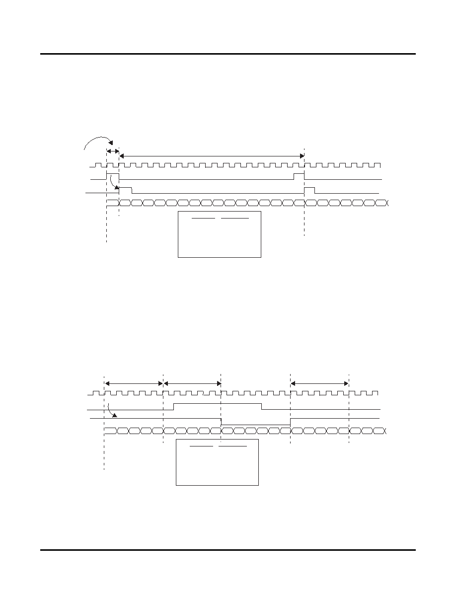
If core FIFO cannot accept cells, cell_begin_ok will be low.
If core FIFO is empty then cell_begin_ok will be asserted every 4 clock cycles until cellvalid is asserted by user
to indicate valid cell data.
cellvalid: Clock-wide pulse asserted by user to indicate valid data. Asserted on the clock cycle following
cell_begin_ok.
Figure 41. ORSO42G5 and ORSO82G5 Transmit FPGA Interface OPC2 Cell Mode
When operating in the eight-link cell mode, the OPC8 block passes user cells from FPGA to embedded core.
Depending upon the congured CELL SIZE, cell transfers will take a variable number of SYSCLK156 cycles to be
transmitted across the interface. Data are always transferred across a 160-bit bus (20 octets per clock cycle).
Figure 42 shows ve clock cycles for a cell transfer this corresponds to a user cell size of 91 octets. The two control
signals in the gure are dened as:
sdo_bp_8: Backpressure signal from core instructing user to stop sending cell data. User should complete trans-
mitting the current cell and can send one more cell before deasserting cellvalid.
cellvalid: Is high throughout a cell transfer to indicate valid cell data
Figure 42. ORSO82G5 Transmit FPGA Interface OPC8 Cell Mode
SYSCLKx[1,2]
cell_begin_ok_x[1,2]
OPC2_x[1,2][39:0]
D
DDD
D
DD
D
DDDD
1 cycle
“n” clk cycles
Cell Size
Clk Cycles
(ocets)
75
79
83
91
16
20
OPC2_x[1,2]_cellvalid
SYSCLK156 8
SDO_BP_8
OPC8[159:0]
D
DDD
D
DD
D
DDDD
“n” clk cycles
Cell Size
Clk Cycles
(ocets)
75
79
83
91
4
5
OPC8_cellvalid
D
“n” clk cycles
相关PDF资料 |
PDF描述 |
|---|---|
| ORT82G5-1FN680I | IC TRANCEIVERS FPSC 680FPBGA |
| ORT82G5-2FN680I | IC TRANCEIVERS FPSC 680FPBGA |
| VI-J4H-IW-F4 | CONVERTER MOD DC/DC 52V 100W |
| VI-J4H-IW-F3 | CONVERTER MOD DC/DC 52V 100W |
| ORT82G5-1FN680C | IC TRANCEIVERS FPSC 680FPBGA |
相关代理商/技术参数 |
参数描述 |
|---|---|
| ORSO42G5-EV | 功能描述:可编程逻辑 IC 开发工具 Eval Brd ORSO42G5 RoHS:否 制造商:Altera Corporation 产品:Development Kits 类型:FPGA 工具用于评估:5CEFA7F3 接口类型: 工作电源电压: |
| ORSO82G5 | 制造商:LATTICE 制造商全称:Lattice Semiconductor 功能描述:0.6 to 2.7 Gbps SONET Backplane Interface FPSCs |
| ORSO82G5-1BM680C | 功能描述:FPGA - 现场可编程门阵列 10368 LUT 372 I/O RoHS:否 制造商:Altera Corporation 系列:Cyclone V E 栅极数量: 逻辑块数量:943 内嵌式块RAM - EBR:1956 kbit 输入/输出端数量:128 最大工作频率:800 MHz 工作电源电压:1.1 V 最大工作温度:+ 70 C 安装风格:SMD/SMT 封装 / 箱体:FBGA-256 |
| ORSO82G5-1BM680I | 功能描述:FPGA - 现场可编程门阵列 10368 LUT 372 I/O RoHS:否 制造商:Altera Corporation 系列:Cyclone V E 栅极数量: 逻辑块数量:943 内嵌式块RAM - EBR:1956 kbit 输入/输出端数量:128 最大工作频率:800 MHz 工作电源电压:1.1 V 最大工作温度:+ 70 C 安装风格:SMD/SMT 封装 / 箱体:FBGA-256 |
| ORSO82G5-1F680C | 功能描述:FPGA - 现场可编程门阵列 ORCA FPSC 2.7GBITS/s BP XCVR 643K RoHS:否 制造商:Altera Corporation 系列:Cyclone V E 栅极数量: 逻辑块数量:943 内嵌式块RAM - EBR:1956 kbit 输入/输出端数量:128 最大工作频率:800 MHz 工作电源电压:1.1 V 最大工作温度:+ 70 C 安装风格:SMD/SMT 封装 / 箱体:FBGA-256 |
发布紧急采购,3分钟左右您将得到回复。