- 您现在的位置:买卖IC网 > PDF目录11733 > ORSO42G5-3BMN484C (Lattice Semiconductor Corporation)IC TRANCEIVERS FPSC 680FPGAM PDF资料下载
参数资料
| 型号: | ORSO42G5-3BMN484C |
| 厂商: | Lattice Semiconductor Corporation |
| 文件页数: | 80/153页 |
| 文件大小: | 0K |
| 描述: | IC TRANCEIVERS FPSC 680FPGAM |
| 产品变化通告: | Product Discontinuation 01/Aug/2011 |
| 标准包装: | 60 |
| 系列: | * |
第1页第2页第3页第4页第5页第6页第7页第8页第9页第10页第11页第12页第13页第14页第15页第16页第17页第18页第19页第20页第21页第22页第23页第24页第25页第26页第27页第28页第29页第30页第31页第32页第33页第34页第35页第36页第37页第38页第39页第40页第41页第42页第43页第44页第45页第46页第47页第48页第49页第50页第51页第52页第53页第54页第55页第56页第57页第58页第59页第60页第61页第62页第63页第64页第65页第66页第67页第68页第69页第70页第71页第72页第73页第74页第75页第76页第77页第78页第79页当前第80页第81页第82页第83页第84页第85页第86页第87页第88页第89页第90页第91页第92页第93页第94页第95页第96页第97页第98页第99页第100页第101页第102页第103页第104页第105页第106页第107页第108页第109页第110页第111页第112页第113页第114页第115页第116页第117页第118页第119页第120页第121页第122页第123页第124页第125页第126页第127页第128页第129页第130页第131页第132页第133页第134页第135页第136页第137页第138页第139页第140页第141页第142页第143页第144页第145页第146页第147页第148页第149页第150页第151页第152页第153页
Lattice Semiconductor
ORCA ORSO42G5 and ORSO82G5 Data Sheet
32
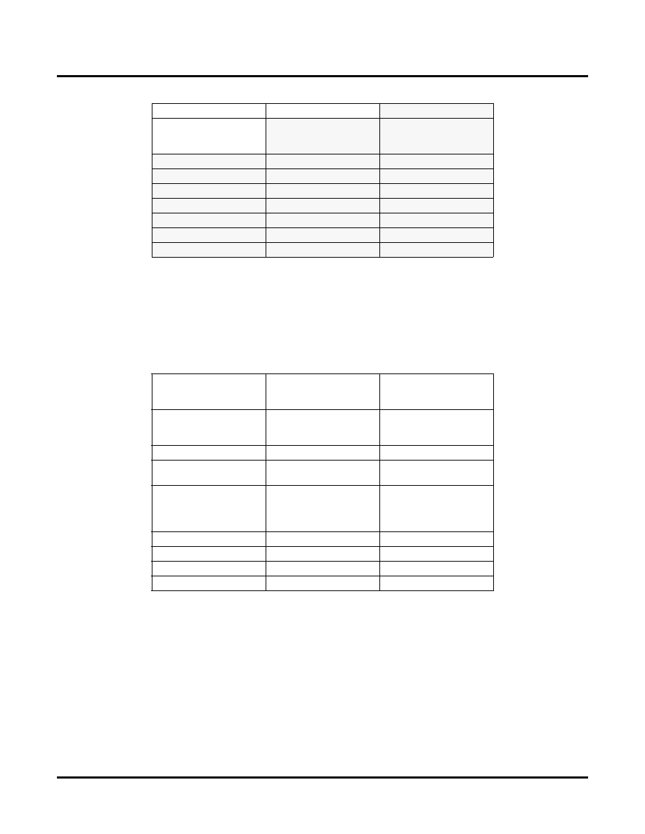
Table 5. Inserted TOH Values (All 0x) in AUTO_SOH Mode
The TOH values inserted in AUTO_SOH mode are shown in Table 5. If a specic value is not listed in the table, the
bytes are transmitted transparently from the FPGA logic as in the transparent mode. Optionally K2 can be inserted
by the core using the FORCE_RDI_xx control register bits. A1/A2 and B1 insertion can be independently enabled.
The TOH values inserted in AUTO_TOH mode are shown in Table 6. The values are for all STS-1s in the STS-48
frame unless noted otherwise.
Table 6. Inserted TOH Values (All 0x) in AUTO_TOH Mode
The TOH block can perform A1/A2 corruption by inverting the A1/A2 bytes and also can forces B1 errors by invert-
ing the B1 byte. A RDI can be injected by forcing the K2 byte to “00000110”. In SONET mode, all TOH bytes can be
transparently sent from the FPGA as an option. Error and RDI insertion are controlled by software register bits as
shown in the Register Map tables.
Scramble Sub-block
The scrambler scrambles the incoming 32-bit data using the standard SONET polynomial 1 + x
6 + x7. The scram-
bler can be disabled by a software register bit.
32:8 MUX
The MUX block is responsible for converting 32 bits of data at 77.76 MHz to 8 bits of data at 311.04 MHz. It will
contain a small elastic store for clock domain transfer between the write clock from the FPGA to the divide-by-4
clock from the SERDES output clock (XCK311). It is recommended to use the clocking scheme shown to guaran-
A1 = F6
A2 = 28
J0
B1 = calculated,
1st. STS-1
B1 = 00, other STS-1s
E1
F1
D1
D2
D3
H1
H2
H3
B2
K1
K2
D4
D5
D6
D7
D8
D9
D10
D11
D12
S1
M1
E2
A1 = F6
A2 = 28
J0 = STS-1 ID,
every 4th. STS-1
J0 = 00, other STS-1s
B1 = calculated,
1st. STS-1
B1 = 00, other STS-1s
E1 = 00
F1 = link number,
1st. STS-1
F1 = 00, other STS-1s
D1 = 00
D2 = 00
D3 = 00
H1 = 62, 1st. STS-1
H1 = 93 other STS-1s
H2 = 0A, 1st. STS-1
H2 = FF other STS-1s
H3 = 00
B2 = 00
K1 = 00
K2 = 06 for RDI,
K2 = 00 otherwise,
1st. STS-1
K2 = 00, other STS-1s
D4 = 00
D5 = 00
D6 = 00
D7 = 00
D8 = 00
D9 = 00
D10 = 00
D11 = 00
D12 = 00
S1 = 00
M1 = 00
E2 = 00
相关PDF资料 |
PDF描述 |
|---|---|
| ORT82G5-1FN680I | IC TRANCEIVERS FPSC 680FPBGA |
| ORT82G5-2FN680I | IC TRANCEIVERS FPSC 680FPBGA |
| VI-J4H-IW-F4 | CONVERTER MOD DC/DC 52V 100W |
| VI-J4H-IW-F3 | CONVERTER MOD DC/DC 52V 100W |
| ORT82G5-1FN680C | IC TRANCEIVERS FPSC 680FPBGA |
相关代理商/技术参数 |
参数描述 |
|---|---|
| ORSO42G5-EV | 功能描述:可编程逻辑 IC 开发工具 Eval Brd ORSO42G5 RoHS:否 制造商:Altera Corporation 产品:Development Kits 类型:FPGA 工具用于评估:5CEFA7F3 接口类型: 工作电源电压: |
| ORSO82G5 | 制造商:LATTICE 制造商全称:Lattice Semiconductor 功能描述:0.6 to 2.7 Gbps SONET Backplane Interface FPSCs |
| ORSO82G5-1BM680C | 功能描述:FPGA - 现场可编程门阵列 10368 LUT 372 I/O RoHS:否 制造商:Altera Corporation 系列:Cyclone V E 栅极数量: 逻辑块数量:943 内嵌式块RAM - EBR:1956 kbit 输入/输出端数量:128 最大工作频率:800 MHz 工作电源电压:1.1 V 最大工作温度:+ 70 C 安装风格:SMD/SMT 封装 / 箱体:FBGA-256 |
| ORSO82G5-1BM680I | 功能描述:FPGA - 现场可编程门阵列 10368 LUT 372 I/O RoHS:否 制造商:Altera Corporation 系列:Cyclone V E 栅极数量: 逻辑块数量:943 内嵌式块RAM - EBR:1956 kbit 输入/输出端数量:128 最大工作频率:800 MHz 工作电源电压:1.1 V 最大工作温度:+ 70 C 安装风格:SMD/SMT 封装 / 箱体:FBGA-256 |
| ORSO82G5-1F680C | 功能描述:FPGA - 现场可编程门阵列 ORCA FPSC 2.7GBITS/s BP XCVR 643K RoHS:否 制造商:Altera Corporation 系列:Cyclone V E 栅极数量: 逻辑块数量:943 内嵌式块RAM - EBR:1956 kbit 输入/输出端数量:128 最大工作频率:800 MHz 工作电源电压:1.1 V 最大工作温度:+ 70 C 安装风格:SMD/SMT 封装 / 箱体:FBGA-256 |
发布紧急采购,3分钟左右您将得到回复。