- 您现在的位置:买卖IC网 > PDF目录11733 > ORSO42G5-3BMN484C (Lattice Semiconductor Corporation)IC TRANCEIVERS FPSC 680FPGAM PDF资料下载
参数资料
| 型号: | ORSO42G5-3BMN484C |
| 厂商: | Lattice Semiconductor Corporation |
| 文件页数: | 11/153页 |
| 文件大小: | 0K |
| 描述: | IC TRANCEIVERS FPSC 680FPGAM |
| 产品变化通告: | Product Discontinuation 01/Aug/2011 |
| 标准包装: | 60 |
| 系列: | * |
第1页第2页第3页第4页第5页第6页第7页第8页第9页第10页当前第11页第12页第13页第14页第15页第16页第17页第18页第19页第20页第21页第22页第23页第24页第25页第26页第27页第28页第29页第30页第31页第32页第33页第34页第35页第36页第37页第38页第39页第40页第41页第42页第43页第44页第45页第46页第47页第48页第49页第50页第51页第52页第53页第54页第55页第56页第57页第58页第59页第60页第61页第62页第63页第64页第65页第66页第67页第68页第69页第70页第71页第72页第73页第74页第75页第76页第77页第78页第79页第80页第81页第82页第83页第84页第85页第86页第87页第88页第89页第90页第91页第92页第93页第94页第95页第96页第97页第98页第99页第100页第101页第102页第103页第104页第105页第106页第107页第108页第109页第110页第111页第112页第113页第114页第115页第116页第117页第118页第119页第120页第121页第122页第123页第124页第125页第126页第127页第128页第129页第130页第131页第132页第133页第134页第135页第136页第137页第138页第139页第140页第141页第142页第143页第144页第145页第146页第147页第148页第149页第150页第151页第152页第153页
Lattice Semiconductor
ORCA ORSO42G5 and ORSO82G5 Data Sheet
108
Absolute Maximum Ratings
Stresses in excess of the absolute maximum ratings can cause permanent damage to the device. These are abso-
lute stress ratings only. Functional operation of the device is not implied at these or any other conditions in excess
of those given in the operations sections of this data sheet. Exposure to absolute maximum ratings for extended
periods can adversely affect device reliability.
The ORCA Series 4 FPSCs include circuitry designed to protect the chips from damaging substrate injection cur-
rents and to prevent accumulations of static charge. Nevertheless, conventional precautions should be observed
during storage, handling, and use to avoid exposure to excessive electrical stress.
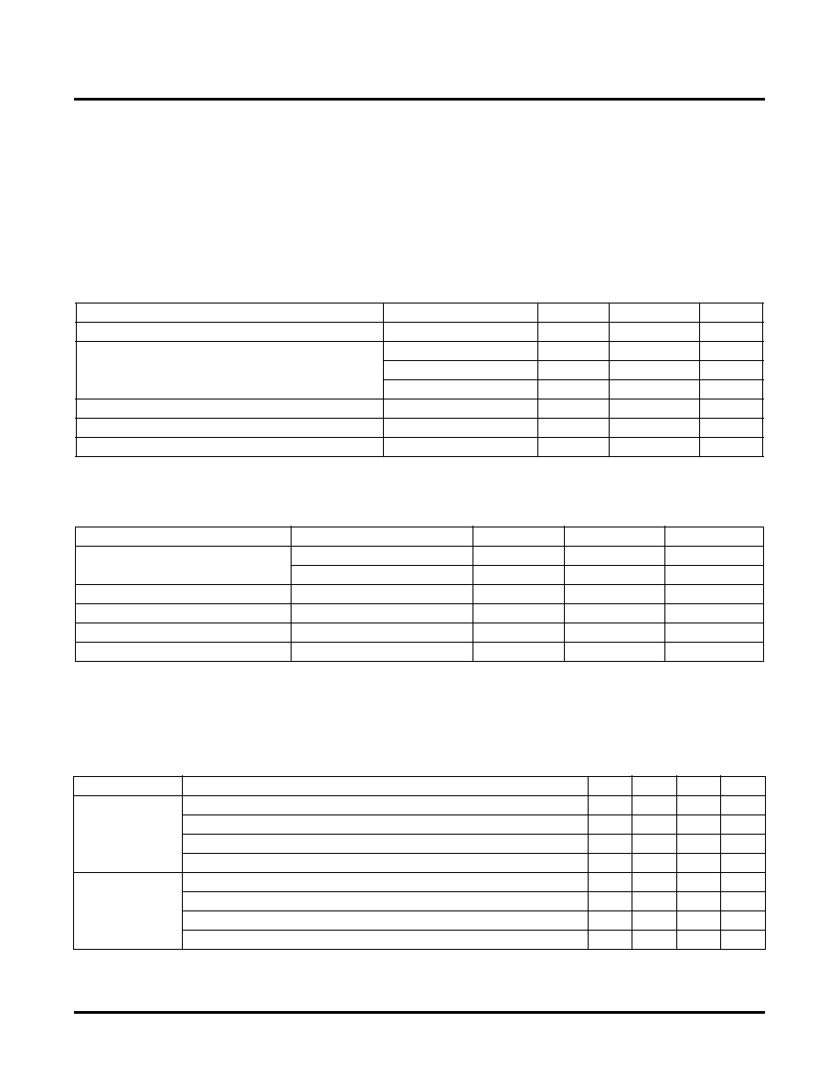
Table 37. Absolute Maximum Ratings
Recommended Operating Conditions
Table 38. Recommended Operating Conditions
SERDES Electrical and Timing Characteristics
Table 39. Maximum Power Dissipation
Parameter
Symbol
Min.
Max.
Units
Storage Temperature
TSTG
-65
150
°C
Power Supply Voltage with Respect to Ground
VDD33
-0.3
4.2
V
VDDIO
-0.3
4.2
V
VDD15, VDD_ANA, VDDGB
-0.3
2.0
V
Input Signal with Respect to Ground
VIN
VSS - 0.3
VDDIO + 0.3
V
Signal Applied to High-Impedance Output
—
VSS - 0.3
VDDIO + 0.3
V
Maximum Package Body (Soldering) Temperature
—
220
°C
Parameter
Symbol
Min.
Max.
Units
Power Supply Voltage
with Respect to Ground
1
VDD33
3.0
3.6
V
VDD15
1.425
1.575
V
Input Voltages
VIN
VSS - 0.3
VDDIO + 0.3
V
Junction Temperature
TJ
-40
125
°C
SERDES Supply Voltage
VDD_ANA, VDDGB
1.425
1.575
V
SERDES CML I/O Supply Voltage
VDDIB, VDDOB
1.425
1.89
V
1. For FPGA Recommended Operating Conditions and Electrical Characteristics, see the Recommended Operating Conditions and Electrical
Characteristics tables in the ORCA Series 4 FPGA data sheet (OR4E04) and technical note TN1036, ORCA Series 4 I/O User’s Guide.
FPSC Standby Currents (IDDSB15 and IDDSB33) are tested with the Embedded Core in the powered down state.
Parameter
Conditions
Min.
Typ.
Max.
1
Units
Power Dissipation
ORSO82G5
SERDES, MUX/DEMUX, Align FIFO and I/O (Per Channel), 1.25 Gbit/s
—
195
mW
SERDES, MUX/DEMUX, Align FIFO and I/O (Per Channel), 2.5 Gbit/s
—
225
mW
Logic Active in Both SONET and Cell Modes (Per Channel)
—
25
mW
Logic Active Only in Cell Mode (Per Channel)
—
10
mW
Power Dissipation
ORSO42G5
SERDES, MUX/DEMUX, Align FIFO and I/O (Per Channel), 1.25 Gbit/s
—
265
mW
SERDES, MUX/DEMUX, Align FIFO and I/O (Per Channel), 2.5 Gbit/s
—
295
mW
Logic Active in Both SONET and Cell Modes (Per Channel)
—
25
mW
Logic Active Only in Cell Mode (Per Channel)
—
10
mW
1. With all channels operating, 1.575V supply.
相关PDF资料 |
PDF描述 |
|---|---|
| ORT82G5-1FN680I | IC TRANCEIVERS FPSC 680FPBGA |
| ORT82G5-2FN680I | IC TRANCEIVERS FPSC 680FPBGA |
| VI-J4H-IW-F4 | CONVERTER MOD DC/DC 52V 100W |
| VI-J4H-IW-F3 | CONVERTER MOD DC/DC 52V 100W |
| ORT82G5-1FN680C | IC TRANCEIVERS FPSC 680FPBGA |
相关代理商/技术参数 |
参数描述 |
|---|---|
| ORSO42G5-EV | 功能描述:可编程逻辑 IC 开发工具 Eval Brd ORSO42G5 RoHS:否 制造商:Altera Corporation 产品:Development Kits 类型:FPGA 工具用于评估:5CEFA7F3 接口类型: 工作电源电压: |
| ORSO82G5 | 制造商:LATTICE 制造商全称:Lattice Semiconductor 功能描述:0.6 to 2.7 Gbps SONET Backplane Interface FPSCs |
| ORSO82G5-1BM680C | 功能描述:FPGA - 现场可编程门阵列 10368 LUT 372 I/O RoHS:否 制造商:Altera Corporation 系列:Cyclone V E 栅极数量: 逻辑块数量:943 内嵌式块RAM - EBR:1956 kbit 输入/输出端数量:128 最大工作频率:800 MHz 工作电源电压:1.1 V 最大工作温度:+ 70 C 安装风格:SMD/SMT 封装 / 箱体:FBGA-256 |
| ORSO82G5-1BM680I | 功能描述:FPGA - 现场可编程门阵列 10368 LUT 372 I/O RoHS:否 制造商:Altera Corporation 系列:Cyclone V E 栅极数量: 逻辑块数量:943 内嵌式块RAM - EBR:1956 kbit 输入/输出端数量:128 最大工作频率:800 MHz 工作电源电压:1.1 V 最大工作温度:+ 70 C 安装风格:SMD/SMT 封装 / 箱体:FBGA-256 |
| ORSO82G5-1F680C | 功能描述:FPGA - 现场可编程门阵列 ORCA FPSC 2.7GBITS/s BP XCVR 643K RoHS:否 制造商:Altera Corporation 系列:Cyclone V E 栅极数量: 逻辑块数量:943 内嵌式块RAM - EBR:1956 kbit 输入/输出端数量:128 最大工作频率:800 MHz 工作电源电压:1.1 V 最大工作温度:+ 70 C 安装风格:SMD/SMT 封装 / 箱体:FBGA-256 |
发布紧急采购,3分钟左右您将得到回复。