- 您现在的位置:买卖IC网 > PDF目录12014 > P89V51RB2BBC,557 (NXP Semiconductors)IC 80C51 MCU 1024 RAM 44TQFP PDF资料下载
参数资料
| 型号: | P89V51RB2BBC,557 |
| 厂商: | NXP Semiconductors |
| 文件页数: | 13/80页 |
| 文件大小: | 0K |
| 描述: | IC 80C51 MCU 1024 RAM 44TQFP |
| 产品培训模块: | Migrating from 8/16-Bit MCUs to 32-Bit ARMs |
| 标准包装: | 800 |
| 系列: | 89V |
| 核心处理器: | 8051 |
| 芯体尺寸: | 8-位 |
| 速度: | 40MHz |
| 连通性: | SPI,UART/USART |
| 外围设备: | 欠压检测/复位,POR,PWM,WDT |
| 输入/输出数: | 32 |
| 程序存储器容量: | 16KB(16K x 8) |
| 程序存储器类型: | 闪存 |
| RAM 容量: | 1K x 8 |
| 电压 - 电源 (Vcc/Vdd): | 4.5 V ~ 5.5 V |
| 振荡器型: | 内部 |
| 工作温度: | 0°C ~ 70°C |
| 封装/外壳: | 44-TQFP |
| 包装: | 托盘 |
| 配用: | 622-1017-ND - BOARD 44-ZIF PLCC SOCKET |
| 其它名称: | 935277723557 P89V51RB2BBC P89V51RB2BBC-ND |
第1页第2页第3页第4页第5页第6页第7页第8页第9页第10页第11页第12页当前第13页第14页第15页第16页第17页第18页第19页第20页第21页第22页第23页第24页第25页第26页第27页第28页第29页第30页第31页第32页第33页第34页第35页第36页第37页第38页第39页第40页第41页第42页第43页第44页第45页第46页第47页第48页第49页第50页第51页第52页第53页第54页第55页第56页第57页第58页第59页第60页第61页第62页第63页第64页第65页第66页第67页第68页第69页第70页第71页第72页第73页第74页第75页第76页第77页第78页第79页第80页
P89V51RB2_RC2_RD2_5
NXP B.V. 2009. All rights reserved.
Product data sheet
Rev. 05 — 12 November 2009
20 of 80
NXP Semiconductors
P89V51RB2/RC2/RD2
8-bit microcontrollers with 80C51 core
6.3 Flash memory IAP
6.3.1 Flash organization
The P89V51RB2/RC2/RD2 program memory consists of a 16/32/64 kB block. ISP
capability, in a second 8 kB block, is provided to allow the user code to be programmed
in-circuit through the serial port. There are three methods of erasing or programming of
the ash memory that may be used. First, the ash may be programmed or erased in the
end-user application by calling low-level routines through a common entry point (IAP).
Second, the on-chip ISP bootloader may be invoked. This ISP bootloader will, in turn, call
low-level routines through the same common entry point that can be used by the end-user
application. Third, the ash may be programmed or erased using the parallel method by
using a commercially available EPROM programmer which supports this device.
6.3.2 Boot block (block 1)
When the microcontroller programs its own ash memory, all of the low level details are
handled by code that is contained in block 1. A user program calls the common entry point
in the block 1 with appropriate parameters to accomplish the desired operation. Boot block
operations include erase user code, program user code, program security bits, etc.
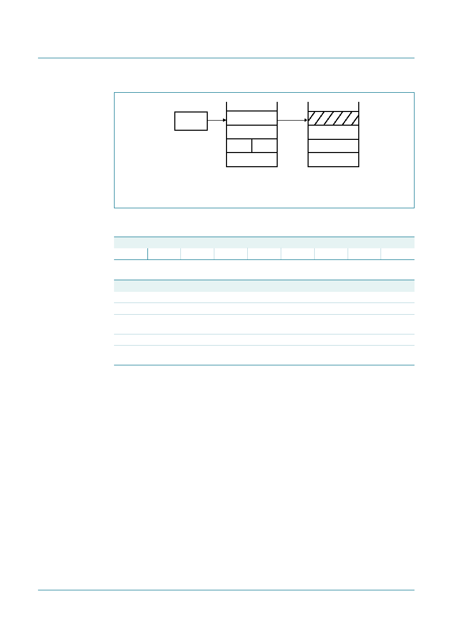
Fig 7.
Dual data pointer organization
Table 10.
AUXR1 - Auxiliary register 1 (address A2H) bit allocation
Not bit addressable; Reset value 00H
Bit
7
6
5
4
3
2
1
0
Symbol
-
GF2
0
-
DPS
Table 11.
AUXR1 - Auxiliary register 1 (address A2H) bit description
Bit
Symbol
Description
7 to 4
-
Reserved for future use. Should be set to ‘0’ by user programs.
3
GF2
General purpose user-dened ag.
2
0
This bit contains a hard-wired ‘0’. Allows toggling of the DPS bit by
incrementing AUXR1, without interfering with other bits in the register.
1
-
Reserved for future use. Should be set to ‘0’ by user programs.
0
DPS
Data pointer select. Chooses one of two Data Pointers for use by the
program. See text for details.
DPL
82H
DPS = 0
→ DPTR0
DPS = 1
→ DPTR1
external data memory
DPS
002aaa518
DPH
83H
DPTR0
DPTR1
AUXR1 / bit0
相关PDF资料 |
PDF描述 |
|---|---|
| VJ1825A223JBCAT4X | CAP CER 0.022UF 200V 5% NP0 1825 |
| VJ1825A223KBCAT4X | CAP CER 0.022UF 200V NP0 1825 |
| VJ2225A562JBAAT4X | CAP CER 5600PF 50V 5% NP0 2225 |
| VJ2225A562JBBAT4X | CAP CER 5600PF 100V 5% NP0 2225 |
| VJ2225A562JBCAT4X | CAP CER 5600PF 200V 5% NP0 2225 |
相关代理商/技术参数 |
参数描述 |
|---|---|
| P89V51RB2FA | 制造商:NXP Semiconductors 功能描述:MCU 8BIT 80C51 16K FLASH PLCC44 |
| P89V51RB2FA,529 | 功能描述:8位微控制器 -MCU 80C51 16K FL / 512 R RoHS:否 制造商:Silicon Labs 核心:8051 处理器系列:C8051F39x 数据总线宽度:8 bit 最大时钟频率:50 MHz 程序存储器大小:16 KB 数据 RAM 大小:1 KB 片上 ADC:Yes 工作电源电压:1.8 V to 3.6 V 工作温度范围:- 40 C to + 105 C 封装 / 箱体:QFN-20 安装风格:SMD/SMT |
| P89V51RB2FA529 | 制造商:NXP Semiconductors 功能描述:IC 8BIT MCU 80C51 40MHZ LCC-44 |
| P89V51RB2FN | 制造商:NXP Semiconductors 功能描述:IC MCU 8BIT 80C51 16K FLASH DIP40 制造商:NXP Semiconductors 功能描述:IC, MCU 8BIT 80C51 16K FLASH, DIP40 |
| P89V51RB2FN,112 | 功能描述:8位微控制器 -MCU 80C51 16K FL / 512 R RoHS:否 制造商:Silicon Labs 核心:8051 处理器系列:C8051F39x 数据总线宽度:8 bit 最大时钟频率:50 MHz 程序存储器大小:16 KB 数据 RAM 大小:1 KB 片上 ADC:Yes 工作电源电压:1.8 V to 3.6 V 工作温度范围:- 40 C to + 105 C 封装 / 箱体:QFN-20 安装风格:SMD/SMT |
发布紧急采购,3分钟左右您将得到回复。