- 您现在的位置:买卖IC网 > PDF目录12014 > P89V51RB2BBC,557 (NXP Semiconductors)IC 80C51 MCU 1024 RAM 44TQFP PDF资料下载
参数资料
| 型号: | P89V51RB2BBC,557 |
| 厂商: | NXP Semiconductors |
| 文件页数: | 53/80页 |
| 文件大小: | 0K |
| 描述: | IC 80C51 MCU 1024 RAM 44TQFP |
| 产品培训模块: | Migrating from 8/16-Bit MCUs to 32-Bit ARMs |
| 标准包装: | 800 |
| 系列: | 89V |
| 核心处理器: | 8051 |
| 芯体尺寸: | 8-位 |
| 速度: | 40MHz |
| 连通性: | SPI,UART/USART |
| 外围设备: | 欠压检测/复位,POR,PWM,WDT |
| 输入/输出数: | 32 |
| 程序存储器容量: | 16KB(16K x 8) |
| 程序存储器类型: | 闪存 |
| RAM 容量: | 1K x 8 |
| 电压 - 电源 (Vcc/Vdd): | 4.5 V ~ 5.5 V |
| 振荡器型: | 内部 |
| 工作温度: | 0°C ~ 70°C |
| 封装/外壳: | 44-TQFP |
| 包装: | 托盘 |
| 配用: | 622-1017-ND - BOARD 44-ZIF PLCC SOCKET |
| 其它名称: | 935277723557 P89V51RB2BBC P89V51RB2BBC-ND |
第1页第2页第3页第4页第5页第6页第7页第8页第9页第10页第11页第12页第13页第14页第15页第16页第17页第18页第19页第20页第21页第22页第23页第24页第25页第26页第27页第28页第29页第30页第31页第32页第33页第34页第35页第36页第37页第38页第39页第40页第41页第42页第43页第44页第45页第46页第47页第48页第49页第50页第51页第52页当前第53页第54页第55页第56页第57页第58页第59页第60页第61页第62页第63页第64页第65页第66页第67页第68页第69页第70页第71页第72页第73页第74页第75页第76页第77页第78页第79页第80页
2009-2011 Microchip Technology Inc.
DS39960D-page 57
PIC18F87K22 FAMILY
4.0
POWER-MANAGED MODES
The PIC18F87K22 family of devices offers a total of
seven operating modes for more efficient power man-
agement. These modes provide a variety of options for
selective power conservation in applications where
resources may be limited (such as battery-powered
devices).
There are three categories of power-managed mode:
Run modes
Idle modes
Sleep mode
There is an Ultra Low-Power Wake-up (ULPWU) for
waking from the Sleep mode.
These categories define which portions of the device
are clocked, and sometimes, at what speed. The Run
and Idle modes may use any of the three available
clock sources (primary, secondary or internal oscillator
block). The Sleep mode does not use a clock source.
The ULPWU mode, on the RA0 pin, enables a slow fall-
ing voltage to generate a wake-up, even from Sleep,
without excess current consumption. (See Section 4.7
The power-managed modes include several power-
saving features offered on previous PIC devices. One
is the clock switching feature, offered in other PIC18
devices. This feature allows the controller to use the
SOSC oscillator instead of the primary one. Another
power-saving feature is Sleep mode, offered by all PIC
devices, where all device clocks are stopped.
4.1
Selecting Power-Managed Modes
Selecting a power-managed mode requires two
decisions:
Will the CPU be clocked or not
What will be the clock source
The IDLEN bit (OSCCON<7>) controls CPU clocking,
while the SCS<1:0> bits (OSCCON<1:0>) select the
clock source. The individual modes, bit settings, clock
sources and affected modules are summarized in
4.1.1
CLOCK SOURCES
The SCS<1:0> bits select one of three clock sources
for power-managed modes. Those sources are:
The primary clock as defined by the FOSC<3:0>
Configuration bits
The secondary clock (the SOSC oscillator)
The internal oscillator block (for LF-INTOSC
modes)
4.1.2
ENTERING POWER-MANAGED
MODES
Switching from one power-managed mode to another
begins by loading the OSCCON register. The
SCS<1:0> bits select the clock source and determine
which Run or Idle mode is used. Changing these bits
causes an immediate switch to the new clock source,
assuming that it is running. The switch may also be
subject to clock transition delays. These considerations
are discussed in Section 4.1.3 “Clock Transitions
and subsequent sections.
Entering the power-managed Idle or Sleep modes is
triggered by the execution of a SLEEP instruction. The
actual mode that results depends on the status of the
IDLEN bit.
Depending on the current and impending mode, a
change to a power-managed mode does not always
require setting all of the previously discussed bits. Many
transitions can be done by changing the oscillator select
bits, or changing the IDLEN bit, prior to issuing a SLEEP
instruction. If the IDLEN bit is already configured as
desired, it may only be necessary to perform a SLEEP
instruction to switch to the desired mode.
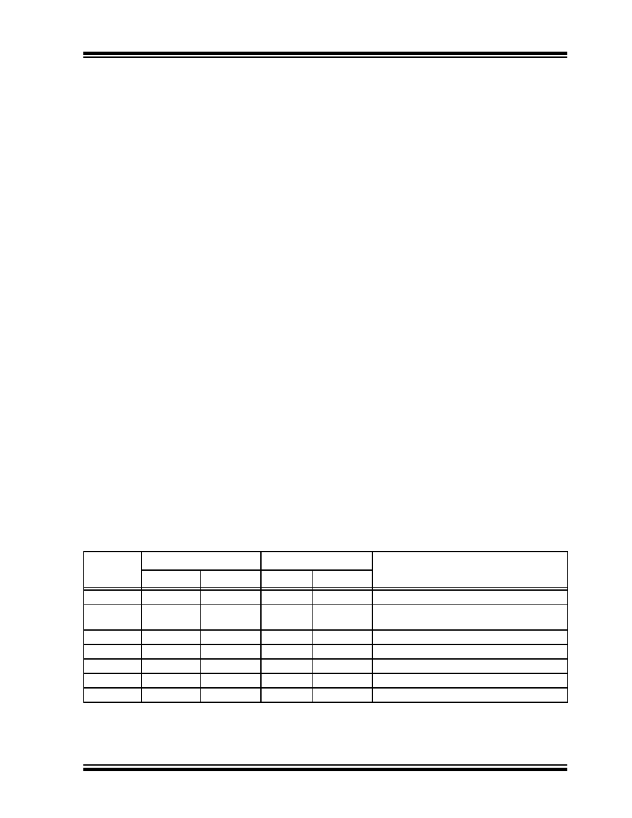
TABLE 4-1:
POWER-MANAGED MODES
Mode
OSCCON Bits
Module Clocking
Available Clock and Oscillator Source
IDLEN<7>(1)
SCS<1:0>
CPU
Peripherals
Sleep
0
N/A
Off
None – All clocks are disabled
PRI_RUN
N/A
00
Clocked
Primary – XT, LP, HS, EC, RC and PLL modes.
This is the normal, Full-Power Execution mode.
SEC_RUN
N/A
01
Clocked
Secondary – SOSC Oscillator
RC_RUN
N/A
1x
Clocked
Internal oscillator block(2)
PRI_IDLE
100
Off
Clocked
Primary – LP, XT, HS, RC, EC
SEC_IDLE
101
Off
Clocked
Secondary – SOSC oscillator
RC_IDLE
11x
Off
Clocked
Internal oscillator block(2)
Note 1:
IDLEN reflects its value when the SLEEP instruction is executed.
2:
Includes INTOSC (HF-INTOSC and MG-INTOSC) and INTOSC postscaler, as well as the LF-INTOSC
source.
相关PDF资料 |
PDF描述 |
|---|---|
| VJ1825A223JBCAT4X | CAP CER 0.022UF 200V 5% NP0 1825 |
| VJ1825A223KBCAT4X | CAP CER 0.022UF 200V NP0 1825 |
| VJ2225A562JBAAT4X | CAP CER 5600PF 50V 5% NP0 2225 |
| VJ2225A562JBBAT4X | CAP CER 5600PF 100V 5% NP0 2225 |
| VJ2225A562JBCAT4X | CAP CER 5600PF 200V 5% NP0 2225 |
相关代理商/技术参数 |
参数描述 |
|---|---|
| P89V51RB2FA | 制造商:NXP Semiconductors 功能描述:MCU 8BIT 80C51 16K FLASH PLCC44 |
| P89V51RB2FA,529 | 功能描述:8位微控制器 -MCU 80C51 16K FL / 512 R RoHS:否 制造商:Silicon Labs 核心:8051 处理器系列:C8051F39x 数据总线宽度:8 bit 最大时钟频率:50 MHz 程序存储器大小:16 KB 数据 RAM 大小:1 KB 片上 ADC:Yes 工作电源电压:1.8 V to 3.6 V 工作温度范围:- 40 C to + 105 C 封装 / 箱体:QFN-20 安装风格:SMD/SMT |
| P89V51RB2FA529 | 制造商:NXP Semiconductors 功能描述:IC 8BIT MCU 80C51 40MHZ LCC-44 |
| P89V51RB2FN | 制造商:NXP Semiconductors 功能描述:IC MCU 8BIT 80C51 16K FLASH DIP40 制造商:NXP Semiconductors 功能描述:IC, MCU 8BIT 80C51 16K FLASH, DIP40 |
| P89V51RB2FN,112 | 功能描述:8位微控制器 -MCU 80C51 16K FL / 512 R RoHS:否 制造商:Silicon Labs 核心:8051 处理器系列:C8051F39x 数据总线宽度:8 bit 最大时钟频率:50 MHz 程序存储器大小:16 KB 数据 RAM 大小:1 KB 片上 ADC:Yes 工作电源电压:1.8 V to 3.6 V 工作温度范围:- 40 C to + 105 C 封装 / 箱体:QFN-20 安装风格:SMD/SMT |
发布紧急采购,3分钟左右您将得到回复。