- 您现在的位置:买卖IC网 > PDF目录12014 > P89V51RB2BBC,557 (NXP Semiconductors)IC 80C51 MCU 1024 RAM 44TQFP PDF资料下载
参数资料
| 型号: | P89V51RB2BBC,557 |
| 厂商: | NXP Semiconductors |
| 文件页数: | 74/80页 |
| 文件大小: | 0K |
| 描述: | IC 80C51 MCU 1024 RAM 44TQFP |
| 产品培训模块: | Migrating from 8/16-Bit MCUs to 32-Bit ARMs |
| 标准包装: | 800 |
| 系列: | 89V |
| 核心处理器: | 8051 |
| 芯体尺寸: | 8-位 |
| 速度: | 40MHz |
| 连通性: | SPI,UART/USART |
| 外围设备: | 欠压检测/复位,POR,PWM,WDT |
| 输入/输出数: | 32 |
| 程序存储器容量: | 16KB(16K x 8) |
| 程序存储器类型: | 闪存 |
| RAM 容量: | 1K x 8 |
| 电压 - 电源 (Vcc/Vdd): | 4.5 V ~ 5.5 V |
| 振荡器型: | 内部 |
| 工作温度: | 0°C ~ 70°C |
| 封装/外壳: | 44-TQFP |
| 包装: | 托盘 |
| 配用: | 622-1017-ND - BOARD 44-ZIF PLCC SOCKET |
| 其它名称: | 935277723557 P89V51RB2BBC P89V51RB2BBC-ND |
第1页第2页第3页第4页第5页第6页第7页第8页第9页第10页第11页第12页第13页第14页第15页第16页第17页第18页第19页第20页第21页第22页第23页第24页第25页第26页第27页第28页第29页第30页第31页第32页第33页第34页第35页第36页第37页第38页第39页第40页第41页第42页第43页第44页第45页第46页第47页第48页第49页第50页第51页第52页第53页第54页第55页第56页第57页第58页第59页第60页第61页第62页第63页第64页第65页第66页第67页第68页第69页第70页第71页第72页第73页当前第74页第75页第76页第77页第78页第79页第80页
PIC18F87K22 FAMILY
DS39960D-page 76
2009-2011 Microchip Technology Inc.
5.5
Configuration Mismatch (CM)
The Configuration Mismatch (CM) Reset is designed to
detect, and attempt to recover from, random, memory
corrupting events. These include Electrostatic Discharge
(ESD) events that can cause widespread, single bit
changes throughout the device and result in catastrophic
failure.
In PIC18F87K22 family Flash devices, the device
Configuration registers (located in the configuration
memory space) are continuously monitored during
operation by comparing their values to complimentary
shadow registers. If a mismatch is detected between
the two sets of registers, a CM Reset automatically
occurs. These events are captured by the CM bit
(RCON<5>). The state of the bit is set to ‘0’ whenever
a CM event occurs and does not change for any other
Reset event.
A CM Reset behaves similarly to a Master Clear Reset,
RESET
instruction, WDT time-out or Stack Event Reset.
As with all hard and power Reset events, the device
Configuration Words are reloaded from the Flash
Configuration Words in program memory as the device
restarts.
5.6
Power-up Timer (PWRT)
PIC18F87K22 family devices incorporate an on-chip
Power-up Timer (PWRT) to help regulate the Power-on
Reset process. The PWRT is enabled by setting the
PWRTEN bit (CONFIG2L<0>). The main function is to
ensure that the device voltage is stable before code is
executed.
The Power-up Timer (PWRT) of the PIC18F87K22
family devices is a 13-bit counter that uses the
LF-INTOSC source as the clock input. This yields an
approximate time interval of 2,048 x 32
s= 66 ms.
While the PWRT is counting, the device is held in
Reset.
The power-up time delay depends on the LF-INTOSC
clock and will vary from chip-to-chip due to temperature
and process variation. See DC Parameter 33 for
details.
5.6.1
TIME-OUT SEQUENCE
If enabled, the PWRT time-out is invoked after the POR
pulse has cleared. The total time-out will vary based on
the status of the PWRT. Figure 5-3, Figure 5-4,
and
all
depict
time-out
sequences on power-up with the Power-up Timer
enabled.
Since the time-outs occur from the POR pulse, if
MCLR is kept low long enough, the PWRT will expire.
Bringing MCLR high will begin execution immediately
(Figure 5-5). This is useful for testing purposes or for
synchronizing more than one PIC18 device operating
in parallel.
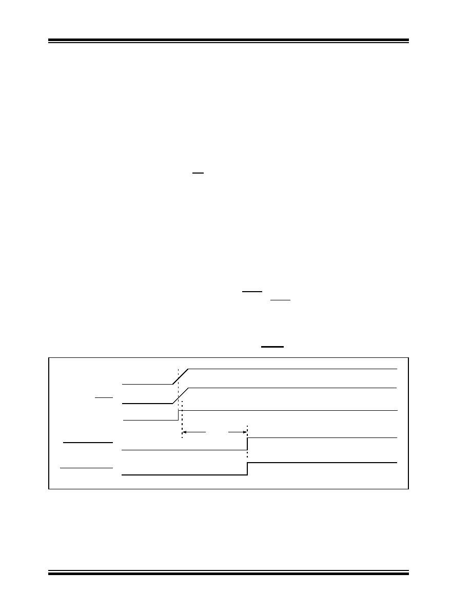
FIGURE 5-3:
TIME-OUT SEQUENCE ON POWER-UP (MCLR TIED TO VDD, VDD RISE < TPWRT)
TPWRT
VDD
MCLR
INTERNAL POR
PWRT TIME-OUT
INTERNAL RESET
相关PDF资料 |
PDF描述 |
|---|---|
| VJ1825A223JBCAT4X | CAP CER 0.022UF 200V 5% NP0 1825 |
| VJ1825A223KBCAT4X | CAP CER 0.022UF 200V NP0 1825 |
| VJ2225A562JBAAT4X | CAP CER 5600PF 50V 5% NP0 2225 |
| VJ2225A562JBBAT4X | CAP CER 5600PF 100V 5% NP0 2225 |
| VJ2225A562JBCAT4X | CAP CER 5600PF 200V 5% NP0 2225 |
相关代理商/技术参数 |
参数描述 |
|---|---|
| P89V51RB2FA | 制造商:NXP Semiconductors 功能描述:MCU 8BIT 80C51 16K FLASH PLCC44 |
| P89V51RB2FA,529 | 功能描述:8位微控制器 -MCU 80C51 16K FL / 512 R RoHS:否 制造商:Silicon Labs 核心:8051 处理器系列:C8051F39x 数据总线宽度:8 bit 最大时钟频率:50 MHz 程序存储器大小:16 KB 数据 RAM 大小:1 KB 片上 ADC:Yes 工作电源电压:1.8 V to 3.6 V 工作温度范围:- 40 C to + 105 C 封装 / 箱体:QFN-20 安装风格:SMD/SMT |
| P89V51RB2FA529 | 制造商:NXP Semiconductors 功能描述:IC 8BIT MCU 80C51 40MHZ LCC-44 |
| P89V51RB2FN | 制造商:NXP Semiconductors 功能描述:IC MCU 8BIT 80C51 16K FLASH DIP40 制造商:NXP Semiconductors 功能描述:IC, MCU 8BIT 80C51 16K FLASH, DIP40 |
| P89V51RB2FN,112 | 功能描述:8位微控制器 -MCU 80C51 16K FL / 512 R RoHS:否 制造商:Silicon Labs 核心:8051 处理器系列:C8051F39x 数据总线宽度:8 bit 最大时钟频率:50 MHz 程序存储器大小:16 KB 数据 RAM 大小:1 KB 片上 ADC:Yes 工作电源电压:1.8 V to 3.6 V 工作温度范围:- 40 C to + 105 C 封装 / 箱体:QFN-20 安装风格:SMD/SMT |
发布紧急采购,3分钟左右您将得到回复。