- 您现在的位置:买卖IC网 > PDF目录269903 > QL5820-33BPTN196C (QUICKLOGIC CORP) PCI BUS CONTROLLER, PBGA196 PDF资料下载
参数资料
| 型号: | QL5820-33BPTN196C |
| 厂商: | QUICKLOGIC CORP |
| 元件分类: | 总线控制器 |
| 英文描述: | PCI BUS CONTROLLER, PBGA196 |
| 封装: | 12 X 12 MM, 1.20 MM HEIGHT, 0.80 MM PITCH, LEAD FREE, PLASTIC, MO-216C, TFBGA-196 |
| 文件页数: | 45/80页 |
| 文件大小: | 1125K |
| 代理商: | QL5820-33BPTN196C |
第1页第2页第3页第4页第5页第6页第7页第8页第9页第10页第11页第12页第13页第14页第15页第16页第17页第18页第19页第20页第21页第22页第23页第24页第25页第26页第27页第28页第29页第30页第31页第32页第33页第34页第35页第36页第37页第38页第39页第40页第41页第42页第43页第44页当前第45页第46页第47页第48页第49页第50页第51页第52页第53页第54页第55页第56页第57页第58页第59页第60页第61页第62页第63页第64页第65页第66页第67页第68页第69页第70页第71页第72页第73页第74页第75页第76页第77页第78页第79页第80页
2006 QuickLogic Corporation
QL58x0 Enhanced QuickPCI Target Family Data Sheet Rev. L
5
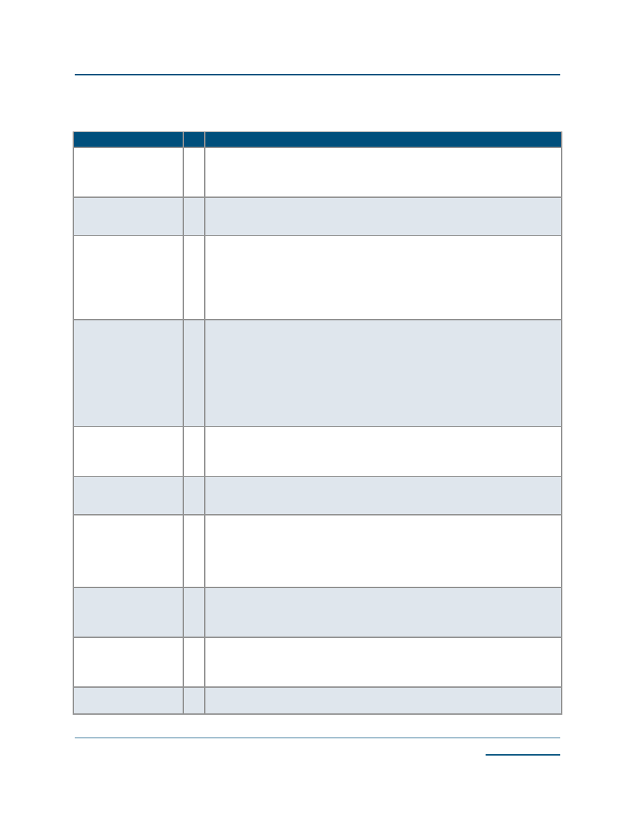
PCI Target Interface
Table 2: PCI Target Interface
Signal
I/O
Description
Usr_Addr_WrData[31:0]
O
Target address, and target Write data. During all target accesses, the address is
presented on Usr_Addr_WrData[31:0]; at the same time, Usr_Adr_Valid is active.
During target Write transactions, this port also presents valid Write data to the PCI
configuration space or user logic when Usr_Adr_Inc is active.
Usr_CBE[3:0]
O
PCI command and byte enables. During target accesses, the PCI command is
presented on Usr_CBE[3:0]; at the same time, Usr_Adr_Valid is active. This port also
presents active-low byte enables to the PCI configuration space or user logic.
Usr_Adr_Valid
O
Indicates the beginning of a PCI transaction, and that a target address is valid on
Usr_Addr_WrData[31:0] and the PCI command is valid on Usr_CBE[3:0]. When this
signal is active, the target address must be latched and decoded to determine if this
address belongs to the device's memory or I/O space. Also, the PCI command must
be decoded to determine the type of PCI transaction. On subsequent clocks of a target
access, this signal is low, indicating that address is NOT present on
Usr_Addr_WrData[31:0].
Usr_Adr_Inc
O
Indicates that the target address should be incremented, because the previous data
transfer has completed. During burst target accesses, the target address is only
presented to the back-end logic at the beginning of the transaction (when
Usr_Adr_Valid is active), and must therefore be latched and incremented by four for
subsequent data transfers. Note that during target Write transactions, Usr_Adr_Inc
indicates valid data on Usr_Addr_WrData[31:0] that must be accepted by the backend
logic (regardless of the state of Usr_Rdy). During Read transactions, Usr_Adr_Inc
signals to the backend that the PCI core has presented the read data on the PCI bus
(TRDYN asserted).
Usr_RdDecode
I
This signal should be the combinatorial decode of the “user read” command from
Usr_CBE[3:0]. This command may be mapped from any of the PCI Read commands,
such as Memory Read, Memory Read Line, Memory Read Multiple, I/O Read, etc. It
is internally gated with Usr_Adr_Valid.
Usr_WrDecode
I
This signal should be the combinatorial decode of the “user write” command from
Usr_CBE[3:0]. This command may be mapped from any of the PCI Write commands,
such as Memory Write or I/O Write. It is internally gated with Usr_Adr_Valid.
Usr_Select
I
This signal should be driven active when the address on Usr_Addr_WrData[31:0] has
been decoded and determined to be within the address space of the device.
Usr_Addr_WrData[31:0] must be compared to each of the valid Base Address
Registers in the PCI configuration space. Also, this signal must be gated by the
Memory Access Enable or I/O Access Enable registers in the PCI configuration space
(Command Register bits 1 or 0 at offset 04h). Internally gated with Usr_Adr_Valid.
Usr_Write
O
This signal is active throughout a “user write” transaction, which has been decoded by
Usr_WrDecode at the beginning of the transaction. The Write strobe for individual
DWORDs of data (on Usr_Addr_WrData[31:0]) during a user Write transaction should
be generated by logically ANDing this signal with Usr_Adr_Inc.
Cfg_Write
O
This signal is active throughout a “configuration write” transaction. The Write strobe
for individual DWORDs of data (on Usr_Addr_WrData[31:0]) during a configuration
Write transaction should be generated by logically ANDing this signal with
Usr_Adr_Inc.
Cfg_RdData[31:0]
I
Data from the PCI configuration registers, required to be presented during PCI
configuration reads.
相关PDF资料 |
PDF描述 |
|---|---|
| QL5842-33BPSN484M | PCI BUS CONTROLLER, PBGA484 |
| QT83C154XXX-L | 8-BIT, MROM, 6 MHz, MICROCONTROLLER, PQFP44 |
| QC87C251SQ | 8-BIT, UVPROM, 12 MHz, MICROCONTROLLER, CDIP40 |
| QR80C51XXX:R | 8-BIT, MROM, 12 MHz, MICROCONTROLLER, CQCC44 |
| QD80C31-S:D | 8-BIT, 20 MHz, MICROCONTROLLER, CDIP40 |
相关代理商/技术参数 |
参数描述 |
|---|---|
| QL5822-33BPTN280C-5695 | 制造商:QuickLogic Corporation 功能描述: |
| QL62506PB516C | 制造商:QUICK LOG 功能描述:New |
| QL6325PQ208 | 制造商:未知厂家 制造商全称:未知厂家 功能描述:ASIC |
| QL6325PT280 | 制造商:未知厂家 制造商全称:未知厂家 功能描述:ASIC |
| QL63D5SA | 制造商:未知厂家 制造商全称:未知厂家 功能描述:InGaAlP Laser Diode |
发布紧急采购,3分钟左右您将得到回复。