- 您现在的位置:买卖IC网 > PDF目录269903 > QL5820-33BPTN196C (QUICKLOGIC CORP) PCI BUS CONTROLLER, PBGA196 PDF资料下载
参数资料
| 型号: | QL5820-33BPTN196C |
| 厂商: | QUICKLOGIC CORP |
| 元件分类: | 总线控制器 |
| 英文描述: | PCI BUS CONTROLLER, PBGA196 |
| 封装: | 12 X 12 MM, 1.20 MM HEIGHT, 0.80 MM PITCH, LEAD FREE, PLASTIC, MO-216C, TFBGA-196 |
| 文件页数: | 8/80页 |
| 文件大小: | 1125K |
| 代理商: | QL5820-33BPTN196C |
第1页第2页第3页第4页第5页第6页第7页当前第8页第9页第10页第11页第12页第13页第14页第15页第16页第17页第18页第19页第20页第21页第22页第23页第24页第25页第26页第27页第28页第29页第30页第31页第32页第33页第34页第35页第36页第37页第38页第39页第40页第41页第42页第43页第44页第45页第46页第47页第48页第49页第50页第51页第52页第53页第54页第55页第56页第57页第58页第59页第60页第61页第62页第63页第64页第65页第66页第67页第68页第69页第70页第71页第72页第73页第74页第75页第76页第77页第78页第79页第80页
2006 QuickLogic Corporation
QL58x0 Enhanced QuickPCI Target Family Data Sheet Rev. L
16
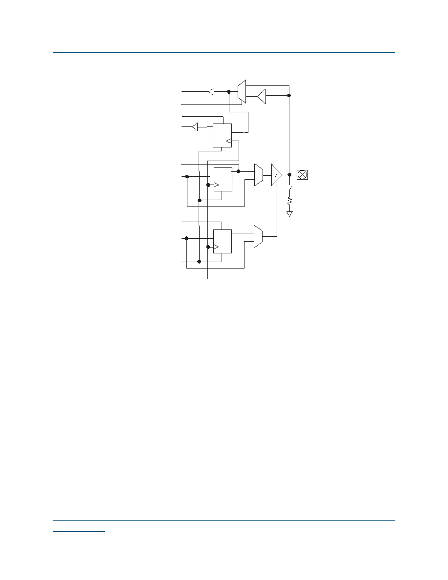
Figure 8: QL58x0 Device Family I/O Cell
The bi-directional I/O pin options can be programmed for input, output, or bi-directional operation. As shown
in Figure 8, each bi-directional I/O pin is associated with an I/O cell which features an input register, an input
buffer, an output register, a three-state output buffer, an output enable register, and 2 two-to-one multiplexers.
The select lines of the two-to-one multiplexers are static and must be connected to either VCC or GND.
For input functions, I/O pins can provide combinatorial, registered data, or both options simultaneously to the
logic array. For combinatorial input operation, data is routed from I/O pins through the input buffer to the
array logic. For registered input operation, I/O pins drive the D input of input cell registers, allowing data to
be captured with fast, predictable set-up times without consuming internal logic cell resources. The comparator
and multiplexer in the input path allows for native support of I/O standards with reference points offset from
traditional ground.
For output functions, I/O pins can receive combinatorial or registered data from the logic array. For
combinatorial output operation, data is routed from the logic array through a multiplexer to the I/O pin. For
registered output operation, the array logic drives the D input of the output cell register which in turn drives
the I/O pin through a multiplexer. The multiplexer allows either a combinatorial or a registered signal to be
driven to the I/O pin. The addition of an output register will also decrease the Tco. Since the output register
does not need to drive the routing the length of the output path is also reduced, and static timing analysis
becomes very predictable.
The three-state output buffer controls the flow of data from the array logic to the I/O pin and allows the I/O
pin to act as an input and/or output. The buffer's output enable can be individually controlled by the logic cell
array or any pin (through the regular routing resources), or it can be bank-controlled through one of the global
networks. The signal can also be either combinatorial or registered. This is identical to that of the flow for the
output cell. For combinatorial control operation, data is routed from the logic array through a multiplexer to
the three-state control. The IOCTRL pins can directly drive the OE and CLK signals for all I/O cells within the
same bank.
E
R
Q
D
R
Q
D
E
R
Q
D
+
-
PAD
OUTPUT ENABLE
REGISTER
OUTPUT
REGISTER
INPUT
REGISTER
相关PDF资料 |
PDF描述 |
|---|---|
| QL5842-33BPSN484M | PCI BUS CONTROLLER, PBGA484 |
| QT83C154XXX-L | 8-BIT, MROM, 6 MHz, MICROCONTROLLER, PQFP44 |
| QC87C251SQ | 8-BIT, UVPROM, 12 MHz, MICROCONTROLLER, CDIP40 |
| QR80C51XXX:R | 8-BIT, MROM, 12 MHz, MICROCONTROLLER, CQCC44 |
| QD80C31-S:D | 8-BIT, 20 MHz, MICROCONTROLLER, CDIP40 |
相关代理商/技术参数 |
参数描述 |
|---|---|
| QL5822-33BPTN280C-5695 | 制造商:QuickLogic Corporation 功能描述: |
| QL62506PB516C | 制造商:QUICK LOG 功能描述:New |
| QL6325PQ208 | 制造商:未知厂家 制造商全称:未知厂家 功能描述:ASIC |
| QL6325PT280 | 制造商:未知厂家 制造商全称:未知厂家 功能描述:ASIC |
| QL63D5SA | 制造商:未知厂家 制造商全称:未知厂家 功能描述:InGaAlP Laser Diode |
发布紧急采购,3分钟左右您将得到回复。