- 您现在的位置:买卖IC网 > PDF目录271227 > S29CL032J0RQAI033 (SPANSION LLC) 1M X 32 FLASH 3.3V PROM, 48 ns, PQFP80 PDF资料下载
参数资料
| 型号: | S29CL032J0RQAI033 |
| 厂商: | SPANSION LLC |
| 元件分类: | PROM |
| 英文描述: | 1M X 32 FLASH 3.3V PROM, 48 ns, PQFP80 |
| 封装: | PLASTIC, MO-108CB-1, QFP-80 |
| 文件页数: | 15/79页 |
| 文件大小: | 2994K |
| 代理商: | S29CL032J0RQAI033 |
第1页第2页第3页第4页第5页第6页第7页第8页第9页第10页第11页第12页第13页第14页当前第15页第16页第17页第18页第19页第20页第21页第22页第23页第24页第25页第26页第27页第28页第29页第30页第31页第32页第33页第34页第35页第36页第37页第38页第39页第40页第41页第42页第43页第44页第45页第46页第47页第48页第49页第50页第51页第52页第53页第54页第55页第56页第57页第58页第59页第60页第61页第62页第63页第64页第65页第66页第67页第68页第69页第70页第71页第72页第73页第74页第75页第76页第77页第78页第79页
22
S29CD-J & S29CL-J Flash Family
S29CD-J_CL-J_00_B3 March 30, 2009
Da ta
Sh e e t
8.
Device Operations
This section describes the read, program, erase, simultaneous read/write operations, and reset features of
the Flash devices.
Operations are initiated by writing specific commands or a sequence with specific address and data patterns
into the command register (see Table 8.1). The command register itself does not occupy any addressable
memory location; rather, it is composed of latches that store the commands, along with the address and data
information needed to execute the command. The contents of the register serve as input to the internal state
machine; the state machine outputs dictate the function of the device. Writing incorrect address and data
values or writing them in an improper sequence may place the device in an unknown state, in which case the
system must write the reset command in order to return the device to the reading array data mode.
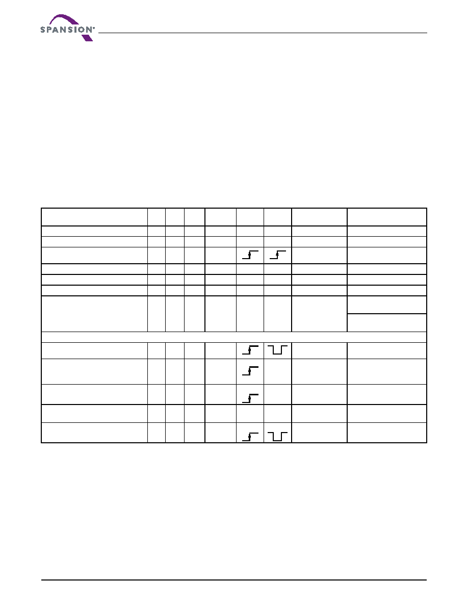
8.1
Device Operation Table
The device must be set up appropriately for each operation. Table 8.1 describes the required state of each
control pin for any particular operation.
Legend
L = Logic Low = VIL, H = Logic High = VIH, X = Don’t care.
Notes
1. WP# controls the two outermost sectors of the top boot block or the two outermost sectors of the bottom boot block.
2. DQ0 reflects the sector PPB (or sector group PPB) and DQ1 reflects the DYB.
Table 8.1 Device Bus Operation
Operation
CE#
OE#
WE#
RESET#
CLK
ADV#
Addresses
Data
(DQ0–DQ31)
Read
L
H
X
AIN
DOUT
Asynchronous Write
L
H
L
H
X
AIN
DIN
Synchronous Write
L
H
L
H
AIN
DIN
Standby (CE#)
H
X
H
X
HIGH Z
Output Disable
L
H
X
HIGH Z
Reset
X
L
X
HIGH Z
PPB Protection Status (Note 2)
L
H
X
Sector Address,
A9 = VID,
A7 – A0 = 02h
00000001h, (protected)
A6 = H
00000000h (unprotect)
A6 = L
Burst Read Operations
Load Starting Burst Address
L
X
H
AIN
X
Advance Burst to next address
with appropriate Data presented
on the Data bus
L
H
X
Burst Data Out
Terminate Current Burst Read Cycle
H
X
H
X
HIGH Z
Terminate Current Burst
Read Cycle with RESET#
XX
H
L
X
HIGH Z
Terminate Current Burst Read Cycle;
Start New Burst Read Cycle
LH
H
AIN
X
相关PDF资料 |
PDF描述 |
|---|---|
| SMCP-67201AV-25SHXXX | 512 X 9 OTHER FIFO, 25 ns, CDIP28 |
| SL0-67201AL-25SB | 512 X 9 OTHER FIFO, 25 ns, UUC28 |
| SL0-67201AL-30MHXXX | 512 X 9 OTHER FIFO, 30 ns, UUC28 |
| SLDP-67201AV-40FHXXX | 512 X 9 OTHER FIFO, 40 ns, CDFP28 |
| SL0-67201AL-40 | 512 X 9 OTHER FIFO, 40 ns, UUC28 |
相关代理商/技术参数 |
参数描述 |
|---|---|
| S29GL016A | 制造商:SPANSION 制造商全称:SPANSION 功能描述:64 Megabit, 32 Megabit, and 16 Megabit 3.0-Volt only Page Mode Flash Memory Featuring 200 nm MirrorBit Process Technology |
| S29GL016A100BAI010 | 制造商:SPANSION 制造商全称:SPANSION 功能描述:64 Megabit, 32 Megabit, and 16 Megabit 3.0-Volt only Page Mode Flash Memory Featuring 200 nm MirrorBit Process Technology |
| S29GL016A100BAI012 | 制造商:SPANSION 制造商全称:SPANSION 功能描述:64 Megabit, 32 Megabit, and 16 Megabit 3.0-Volt only Page Mode Flash Memory Featuring 200 nm MirrorBit Process Technology |
| S29GL016A100BAI013 | 制造商:SPANSION 制造商全称:SPANSION 功能描述:64 Megabit, 32 Megabit, and 16 Megabit 3.0-Volt only Page Mode Flash Memory Featuring 200 nm MirrorBit Process Technology |
| S29GL016A100BAIR10 | 制造商:SPANSION 制造商全称:SPANSION 功能描述:64 Megabit, 32 Megabit, and 16 Megabit 3.0-Volt only Page Mode Flash Memory Featuring 200 nm MirrorBit Process Technology |
发布紧急采购,3分钟左右您将得到回复。