- 您现在的位置:买卖IC网 > PDF目录271227 > S29CL032J0RQAI033 (SPANSION LLC) 1M X 32 FLASH 3.3V PROM, 48 ns, PQFP80 PDF资料下载
参数资料
| 型号: | S29CL032J0RQAI033 |
| 厂商: | SPANSION LLC |
| 元件分类: | PROM |
| 英文描述: | 1M X 32 FLASH 3.3V PROM, 48 ns, PQFP80 |
| 封装: | PLASTIC, MO-108CB-1, QFP-80 |
| 文件页数: | 24/79页 |
| 文件大小: | 2994K |
| 代理商: | S29CL032J0RQAI033 |
第1页第2页第3页第4页第5页第6页第7页第8页第9页第10页第11页第12页第13页第14页第15页第16页第17页第18页第19页第20页第21页第22页第23页当前第24页第25页第26页第27页第28页第29页第30页第31页第32页第33页第34页第35页第36页第37页第38页第39页第40页第41页第42页第43页第44页第45页第46页第47页第48页第49页第50页第51页第52页第53页第54页第55页第56页第57页第58页第59页第60页第61页第62页第63页第64页第65页第66页第67页第68页第69页第70页第71页第72页第73页第74页第75页第76页第77页第78页第79页
30
S29CD-J & S29CL-J Flash Family
S29CD-J_CL-J_00_B3 March 30, 2009
Da ta
Sh e e t
8.7.1
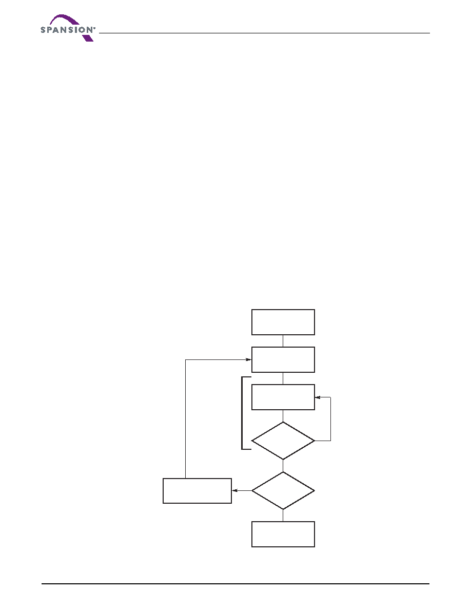
Programming
Programming is a four-bus-cycle operation. The program command sequence is initiated by writing two
unlock write cycles, followed by the program setup command. The program address and data are written
next, which in turn initiate the Embedded Program algorithm. The system is not required to provide further
controls or timings. The device automatically generates the program pulses and verifies the programmed cell
margin. Section 20.1, Command Definitions on page 73 shows the address and data requirements for the
program command sequence.
Note the following:
When the Embedded Program algorithm is complete, the device returns to the read mode and address are
no longer latched. An address change is required to begin reading valid array data.
The system can determine the status of the program operation by using DQ7, DQ6 or RY/BY#. Refer to
Section 8.8, Write Operation Status on page 34 for information on these status bits.
A “0” cannot be programmed back to a “1.” Attempting to do so may halt the operation and set DQ5 to 1, or
cause the Data# Polling algorithm to indicate the operation was successful.. A succeeding read shows that
the data is still “0.” Only erase operations can convert a “0” to a “1.”
Any commands written to the device during the Embedded Program Algorithm are ignored except the
Program Suspend command.
A hardware reset immediately terminates the program operation; the program command sequence should
be re-initiated once the device has returned to the read mode, to ensure data integrity.
For the 32Mb S29CD-J and S29CL-J devices only:
Please refer to the application note “Recommended Mode of Operation for Spansion 110 nm
S29CD032J/S29CL032J Flash Memory” publication number S29CD-CL032J_Recommend_AN for
programming best practices.
Figure 8.5 Program Operation
Note
See Table 19.1 and Table 20.2 for program command sequence.
START
Write Program
Command Sequence
Data Poll
from System
Verify Data?
No
Yes
Last Address?
No
Yes
Programming
Completed
Increment Address
Embedded
Program
algorithm
in progress
相关PDF资料 |
PDF描述 |
|---|---|
| SMCP-67201AV-25SHXXX | 512 X 9 OTHER FIFO, 25 ns, CDIP28 |
| SL0-67201AL-25SB | 512 X 9 OTHER FIFO, 25 ns, UUC28 |
| SL0-67201AL-30MHXXX | 512 X 9 OTHER FIFO, 30 ns, UUC28 |
| SLDP-67201AV-40FHXXX | 512 X 9 OTHER FIFO, 40 ns, CDFP28 |
| SL0-67201AL-40 | 512 X 9 OTHER FIFO, 40 ns, UUC28 |
相关代理商/技术参数 |
参数描述 |
|---|---|
| S29GL016A | 制造商:SPANSION 制造商全称:SPANSION 功能描述:64 Megabit, 32 Megabit, and 16 Megabit 3.0-Volt only Page Mode Flash Memory Featuring 200 nm MirrorBit Process Technology |
| S29GL016A100BAI010 | 制造商:SPANSION 制造商全称:SPANSION 功能描述:64 Megabit, 32 Megabit, and 16 Megabit 3.0-Volt only Page Mode Flash Memory Featuring 200 nm MirrorBit Process Technology |
| S29GL016A100BAI012 | 制造商:SPANSION 制造商全称:SPANSION 功能描述:64 Megabit, 32 Megabit, and 16 Megabit 3.0-Volt only Page Mode Flash Memory Featuring 200 nm MirrorBit Process Technology |
| S29GL016A100BAI013 | 制造商:SPANSION 制造商全称:SPANSION 功能描述:64 Megabit, 32 Megabit, and 16 Megabit 3.0-Volt only Page Mode Flash Memory Featuring 200 nm MirrorBit Process Technology |
| S29GL016A100BAIR10 | 制造商:SPANSION 制造商全称:SPANSION 功能描述:64 Megabit, 32 Megabit, and 16 Megabit 3.0-Volt only Page Mode Flash Memory Featuring 200 nm MirrorBit Process Technology |
发布紧急采购,3分钟左右您将得到回复。