- 您现在的位置:买卖IC网 > PDF目录271227 > S29CL032J0RQAI033 (SPANSION LLC) 1M X 32 FLASH 3.3V PROM, 48 ns, PQFP80 PDF资料下载
参数资料
| 型号: | S29CL032J0RQAI033 |
| 厂商: | SPANSION LLC |
| 元件分类: | PROM |
| 英文描述: | 1M X 32 FLASH 3.3V PROM, 48 ns, PQFP80 |
| 封装: | PLASTIC, MO-108CB-1, QFP-80 |
| 文件页数: | 39/79页 |
| 文件大小: | 2994K |
| 代理商: | S29CL032J0RQAI033 |
第1页第2页第3页第4页第5页第6页第7页第8页第9页第10页第11页第12页第13页第14页第15页第16页第17页第18页第19页第20页第21页第22页第23页第24页第25页第26页第27页第28页第29页第30页第31页第32页第33页第34页第35页第36页第37页第38页当前第39页第40页第41页第42页第43页第44页第45页第46页第47页第48页第49页第50页第51页第52页第53页第54页第55页第56页第57页第58页第59页第60页第61页第62页第63页第64页第65页第66页第67页第68页第69页第70页第71页第72页第73页第74页第75页第76页第77页第78页第79页
44
S29CD-J & S29CL-J Flash Family
S29CD-J_CL-J_00_B3 March 30, 2009
Da ta
Sh e e t
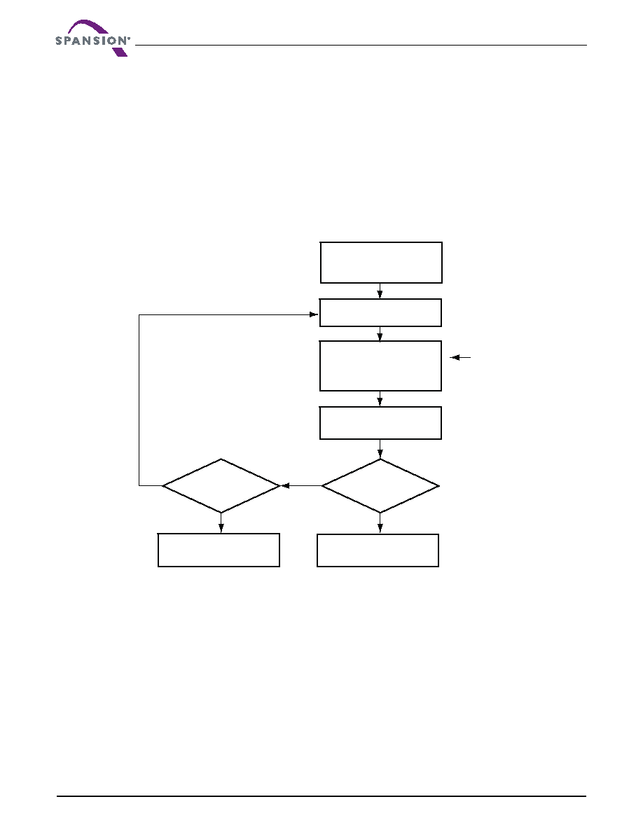
9.2.1
Programming PPB
The PPB Program Command is used to program, or set, a given PPB. The first three cycles in the PPB
Program Command are standard unlock cycles. The fourth cycle in the PPB Program Command executes the
pulse which programs the specified PPB. The user must wait either 100 s or until DQ6 stops toggling before
executing the fifth cycle, which is the read verify portion of the PPB Program Command. The sixth cycle
outputs the status of the PPB Program operation.
In the event that the program PPB operation was not successful, the user can loop directly to the fourth cycle
of the PPB Program Command to perform the program pulse and read verification again. After four
unsuccessful loops through the program pulse and read verification cycles the PPB programming operation
should be considered a failure.
Figure 9.2 PPB Program Operation
9.2.2
Erasing PPB
The All PPB Erase command is used to erase all the PPBs in bulk. There are no means for individually
erasing a specific PPB. The first three cycles of the PPB Erase command are standard unlock cycles. The
fourth cycle executes the erase pulse to all the PPBs. The user must wait either 20ms or until DQ6 stops
toggling before executing the fifth cycle, which is the read verify portion of the PPB Erase Command. The
sixth cycle outputs the status of the PPB Erase operation.
In the event that the erase PPB operation was not successful, the user can loop directly to the fourth cycle of
the All PPB Erase Command to perform the erase pulse and read verification again. After four unsuccessful
loops through the erase pulse and read verification cycles, the PPB erasing operation should be considered a
failure.
Note
All PPB must be preprogrammed prior to issuing the All PPB Erase Command.
Either poll DQ6 in the
small bank and wait for
it to stop toggling OR
wait 100
s
DQ0 = 1?
Write 0x68 to SG+WP
Write 0x48 to SG+WP
Read from SG+WP
YES
NO
YES
NO
Done
Error
Write 0xAA to 0x555
Write 0x55 to 0x2AA
Write 0x60 to 0x555
5th attempt?
Note: Reads from the
small bank at this point
return the status of the
operation, not read array
data.
相关PDF资料 |
PDF描述 |
|---|---|
| SMCP-67201AV-25SHXXX | 512 X 9 OTHER FIFO, 25 ns, CDIP28 |
| SL0-67201AL-25SB | 512 X 9 OTHER FIFO, 25 ns, UUC28 |
| SL0-67201AL-30MHXXX | 512 X 9 OTHER FIFO, 30 ns, UUC28 |
| SLDP-67201AV-40FHXXX | 512 X 9 OTHER FIFO, 40 ns, CDFP28 |
| SL0-67201AL-40 | 512 X 9 OTHER FIFO, 40 ns, UUC28 |
相关代理商/技术参数 |
参数描述 |
|---|---|
| S29GL016A | 制造商:SPANSION 制造商全称:SPANSION 功能描述:64 Megabit, 32 Megabit, and 16 Megabit 3.0-Volt only Page Mode Flash Memory Featuring 200 nm MirrorBit Process Technology |
| S29GL016A100BAI010 | 制造商:SPANSION 制造商全称:SPANSION 功能描述:64 Megabit, 32 Megabit, and 16 Megabit 3.0-Volt only Page Mode Flash Memory Featuring 200 nm MirrorBit Process Technology |
| S29GL016A100BAI012 | 制造商:SPANSION 制造商全称:SPANSION 功能描述:64 Megabit, 32 Megabit, and 16 Megabit 3.0-Volt only Page Mode Flash Memory Featuring 200 nm MirrorBit Process Technology |
| S29GL016A100BAI013 | 制造商:SPANSION 制造商全称:SPANSION 功能描述:64 Megabit, 32 Megabit, and 16 Megabit 3.0-Volt only Page Mode Flash Memory Featuring 200 nm MirrorBit Process Technology |
| S29GL016A100BAIR10 | 制造商:SPANSION 制造商全称:SPANSION 功能描述:64 Megabit, 32 Megabit, and 16 Megabit 3.0-Volt only Page Mode Flash Memory Featuring 200 nm MirrorBit Process Technology |
发布紧急采购,3分钟左右您将得到回复。