- 您现在的位置:买卖IC网 > PDF目录16215 > SI3225DC0-EVB (Silicon Laboratories Inc)DAUGHTER CARD W/SI3200 INTERFACE PDF资料下载
参数资料
| 型号: | SI3225DC0-EVB |
| 厂商: | Silicon Laboratories Inc |
| 文件页数: | 66/112页 |
| 文件大小: | 0K |
| 描述: | DAUGHTER CARD W/SI3200 INTERFACE |
| 标准包装: | 1 |
| 系列: | ProSLIC® |
| 主要目的: | 接口,模拟前端(AFE) |
| 已用 IC / 零件: | Si3225 |
| 已供物品: | 板,CD |
第1页第2页第3页第4页第5页第6页第7页第8页第9页第10页第11页第12页第13页第14页第15页第16页第17页第18页第19页第20页第21页第22页第23页第24页第25页第26页第27页第28页第29页第30页第31页第32页第33页第34页第35页第36页第37页第38页第39页第40页第41页第42页第43页第44页第45页第46页第47页第48页第49页第50页第51页第52页第53页第54页第55页第56页第57页第58页第59页第60页第61页第62页第63页第64页第65页当前第66页第67页第68页第69页第70页第71页第72页第73页第74页第75页第76页第77页第78页第79页第80页第81页第82页第83页第84页第85页第86页第87页第88页第89页第90页第91页第92页第93页第94页第95页第96页第97页第98页第99页第100页第101页第102页第103页第104页第105页第106页第107页第108页第109页第110页第111页第112页
Si3220/25 Si3200/02
Rev. 1.3
57
Not
Recommended
fo
r N
ew
D
esi
gn
s
The Si3220 can also add a dc offset component to the
ringing signal and detect a ring trip event by monitoring
the dc loop current flowing once the terminal equipment
transitions to the off-hook state. Although adding dc
offset reduces the maximum available ringing amplitude
(using the same ringing supply), this method is required
to reliably detect a valid ring trip event when sourcing
longer loop lengths. The dc offset can be programmed
from 0 to 64.32 V in the RINGOF RAM address as
required to produce adequate dc loop current in the off-
hook state. Depending on the loop length and the ring
trip method, the ac or dc ring trip detection circuits are
disabled by setting their respective ring trip thresholds,
RTACTH or RTDCTH, sufficiently high so that they do
not trip under any condition.
3.15.5. Si3225 Ring Trip Detection
The Si3225 implements an external ring trip detection
scheme when using a standard battery-backed external
ringing generator. In this application, the centralized
ringing generator produces an unbalanced ringing
signal that is distributed to individual TIP/RING pairs. A
per-channel ringing relay is required to disconnect the
Si3225 from the TIP/RING pair and apply the ringing
signal. By monitoring the ringing feed path across a ring
series with the ringing source, the Si3225 can detect the
dc current path created when the hook switch inside the
terminal equipment closes. The internal ring trip
detection circuitry is identical to that illustrated in
Figure 27. Figure 31 illustrates the typical external ring
trip circuitry required for the Si3225. Because of the
long loop nature of these applications, a dc ring trip
detection scheme is typically used. The user can
disable the ac ring trip detection circuitry by setting the
RTACTH threshold sufficiently high so it does not trip
under any condition.
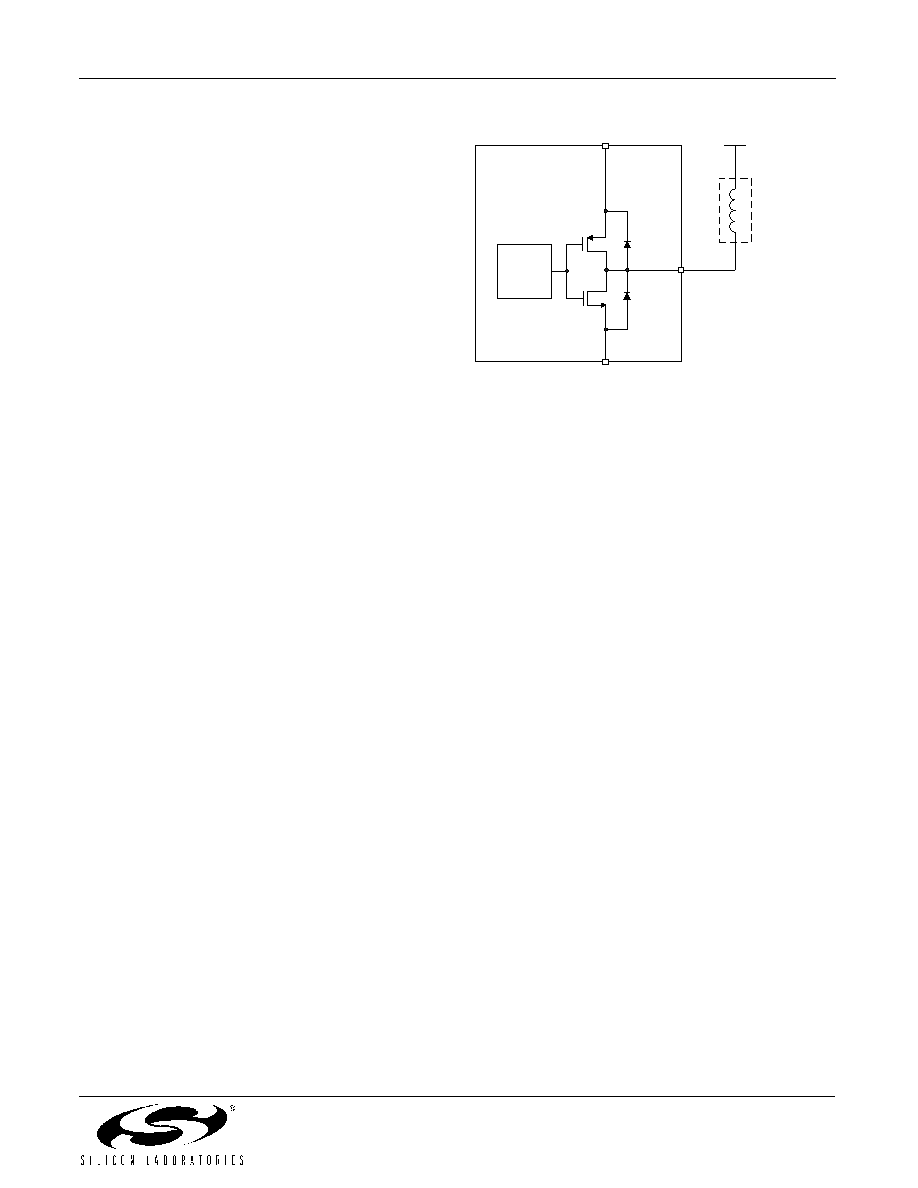
3.16. Relay Driver Considerations
The Dual ProSLIC devices include up to three
dedicated relay drivers to drive external ringing and/or
test relays. Test relay drivers TRD1a, TRD1b, TRD2a,
and TRD2b are provided in all product versions, and
ringing relay drivers RRDa and RRDb are included for
the Si3225 only. In most applications, the relay can be
driven directly from the Dual ProSLIC with no external
relay drive circuitry required. Figure 28 illustrates the
internal relay driver circuitry using a 3 V or 5 V relay.
Figure 28. Dual ProSLIC Internal Relay Drive
Circuitry
The internal driver logic and drive circuitry are powered
by the same VDD supply as the chip’s main VDD supply
(VDD1–VDD4 pins). When operating external relays from
a VCC supply equal to the chip’s VDD supply, an internal
diode network provides protection against overvoltage
conditions from flyback spikes when the relay is
opened. Either 3 V or 5 V relays can be used in the
configuration shown in Figure 28, and either polarized
or non-polarized relays are acceptable if the VCC and
VDD supplies are identical. The input impedance, RIN, of
the relay driver pins is a constant 11
while sinking
less than the maximum rated 85 mA into the pin.
If the operating voltage of the relay (VCC) is higher than
the Dual ProSLIC VDD supply voltage, an external drive
circuit is required to eliminate leakage from VCC to VDD
through
the
internal
protection
diode.
In
this
configuration, a polarized relay will provide optimal
overvoltage
protection
and
minimal
external
components. Figure 29 illustrates the required external
drive circuit, and Table 32 provides recommended
values for RDRV for typical relay characteristics and VCC
supplies. The output impedance, ROUT, of the relay
driver pins is a constant 63
while sourcing less than
the maximum rated 28 mA out of the pin.
Si3220/
Si3225
Relay
Driver
Logic
V
DD
GDD
RRDa/b
TRD1a/b
TRD2a/b
V
CC
3 V/5 V Relay
(polarized or
non-polarized)
相关PDF资料 |
PDF描述 |
|---|---|
| SEK220M400ST | CAP ALUM 22UF 400V 20% RADIAL |
| CP2201EK | KIT EVAL FOR CP2201 ETH CTRLR |
| PM1210-820J-RC | INDUCTOR 82UH 5% 1210 SMD |
| H3WWH-6036G | IDC CABLE - HPL60H/AE60G/HPL60H |
| UPS2C471MRD | CAP ALUM 470UF 160V 20% RADIAL |
相关代理商/技术参数 |
参数描述 |
|---|---|
| SI3225DCX-EVB | 功能描述:子卡和OEM板 Si3225 Daughter Card RoHS:否 制造商:BeagleBoard by CircuitCo 产品:BeagleBone LCD4 Boards 用于:BeagleBone - BB-Bone - Open Source Development Kit |
| Si3225-FQ | 功能描述:电信线路管理 IC Dual-Channel SLIC/ codec RoHS:否 制造商:STMicroelectronics 产品:PHY 接口类型:UART 电源电压-最大:18 V 电源电压-最小:8 V 电源电流:30 mA 最大工作温度:+ 85 C 最小工作温度:- 40 C 安装风格:SMD/SMT 封装 / 箱体:VFQFPN-48 封装:Tray |
| SI3225-FQR | 制造商:Silicon Laboratories Inc 功能描述: |
| Si3225-G-FQ | 功能描述:电信线路管理 IC Dual-Channel SLIC codec RoHS:否 制造商:STMicroelectronics 产品:PHY 接口类型:UART 电源电压-最大:18 V 电源电压-最小:8 V 电源电流:30 mA 最大工作温度:+ 85 C 最小工作温度:- 40 C 安装风格:SMD/SMT 封装 / 箱体:VFQFPN-48 封装:Tray |
| SI3225-G-FQR | 功能描述:电信线路管理 IC Dual-CH SLIC/codec Ext Ringing Support RoHS:否 制造商:STMicroelectronics 产品:PHY 接口类型:UART 电源电压-最大:18 V 电源电压-最小:8 V 电源电流:30 mA 最大工作温度:+ 85 C 最小工作温度:- 40 C 安装风格:SMD/SMT 封装 / 箱体:VFQFPN-48 封装:Tray |
发布紧急采购,3分钟左右您将得到回复。