- 您现在的位置:买卖IC网 > PDF目录16215 > SI3225DC0-EVB (Silicon Laboratories Inc)DAUGHTER CARD W/SI3200 INTERFACE PDF资料下载
参数资料
| 型号: | SI3225DC0-EVB |
| 厂商: | Silicon Laboratories Inc |
| 文件页数: | 88/112页 |
| 文件大小: | 0K |
| 描述: | DAUGHTER CARD W/SI3200 INTERFACE |
| 标准包装: | 1 |
| 系列: | ProSLIC® |
| 主要目的: | 接口,模拟前端(AFE) |
| 已用 IC / 零件: | Si3225 |
| 已供物品: | 板,CD |
第1页第2页第3页第4页第5页第6页第7页第8页第9页第10页第11页第12页第13页第14页第15页第16页第17页第18页第19页第20页第21页第22页第23页第24页第25页第26页第27页第28页第29页第30页第31页第32页第33页第34页第35页第36页第37页第38页第39页第40页第41页第42页第43页第44页第45页第46页第47页第48页第49页第50页第51页第52页第53页第54页第55页第56页第57页第58页第59页第60页第61页第62页第63页第64页第65页第66页第67页第68页第69页第70页第71页第72页第73页第74页第75页第76页第77页第78页第79页第80页第81页第82页第83页第84页第85页第86页第87页当前第88页第89页第90页第91页第92页第93页第94页第95页第96页第97页第98页第99页第100页第101页第102页第103页第104页第105页第106页第107页第108页第109页第110页第111页第112页
Si3220/25 Si3200/02
Rev. 1.3
77
Not
Recommended
fo
r N
ew
D
esi
gn
s
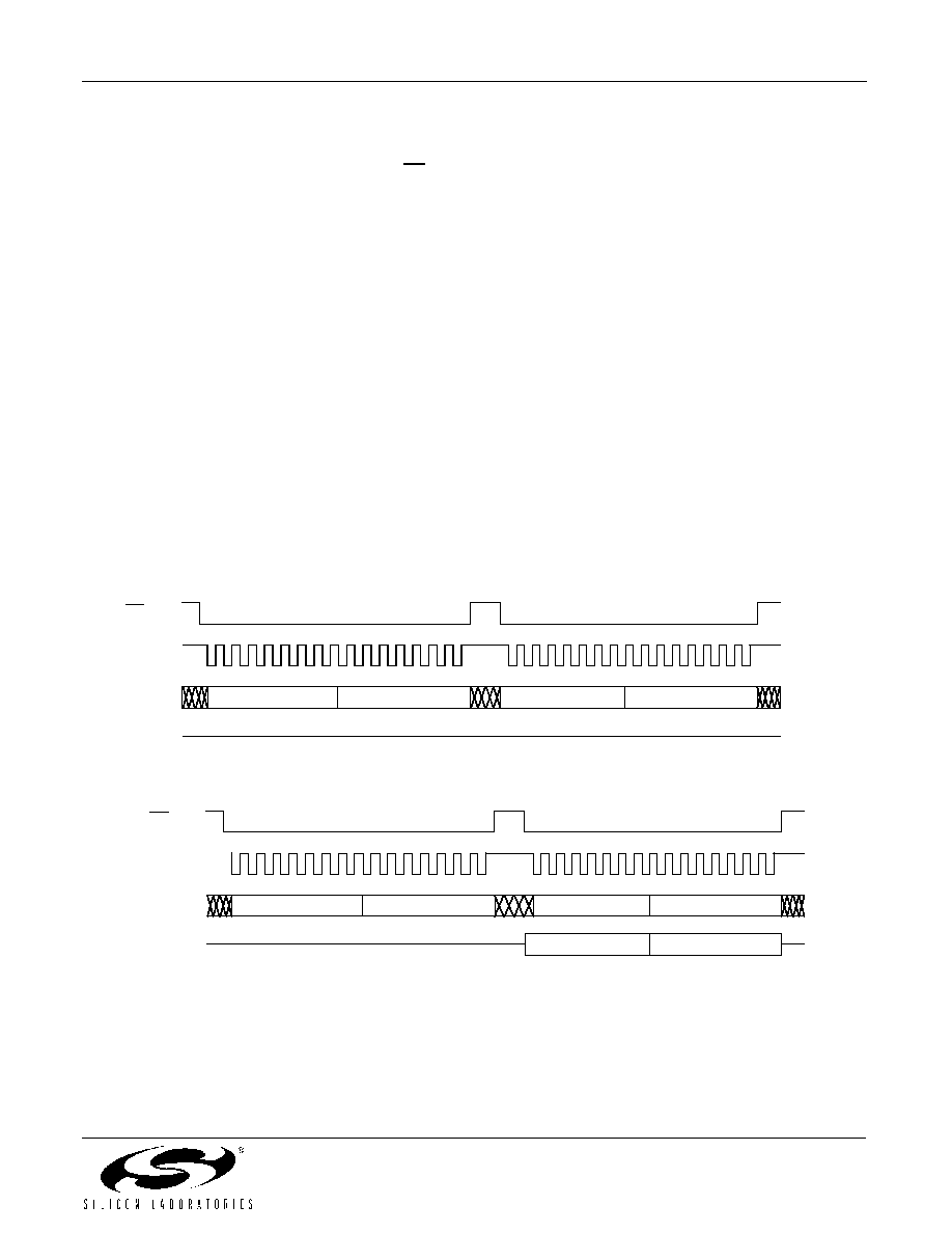
operations to register addresses via a 16-bit SPI
controller. These operations require a 4-byte transfer
arranged as two 16-bit words. The absence of CS going
high after the eighth bit of data indicates to the SPI state
machine that eight more SCLK pulses follow to
complete the operation. For a WRITE operation, the last
eight bits are ignored. For a read operation, the 8-bit
data value repeats so that the data is captured during
the last half of a data transfer if required by the
controller.
During register accesses, the CONTROL, ADDRESS,
and DATA are captured in the SPI module. At the
completion of the ADDRESS byte of a READ access,
the contents of the addressed register move into the
data register of the SPI data register. At the completion
of the DATA byte of a WRITE access, the data is
transferred from the SPI to the addressed register.
Figures 47–50 illustrate the various cycles for accessing
RAM addresses. RAM addresses are 16-bit entities;
therefore, the accesses always require four bytes.
During
RAM
address
accesses,
the
CONTROL,
ADDRESS, and DATA are captured in the SPI module.
At the completion of the ADDRESS byte of a READ
access, the contents of the channel-based data buffer
move into the data register in the SPI for shifting out
during the DATA portion of the SPI transfer. This is the
data loaded into the data buffer in response to the
previous RAM address read request. Therefore, there is
a one-deep pipeline nature to RAM address READ
operations. At the completion of the DATA portion of the
READ cycle, the ADDRESS is transferred to the
channel-based address buffer register, and a RAM
address is logged for that channel. The RAMSTAT bit in
each channel is polled to monitor the status of RAM
address accesses that are serviced twice per sample
period at dedicated windows in the DSP algorithm.
A RAM access interrupt in each channel indicates that
the pending RAM access request is serviced. For a
RAM access, the ADDRESS and DATA is transferred
from the SPI registers to the address and data buffers in
the appropriate channel. The RAM WRITE request is
logged. As for READ operations, the status of the
pending request is monitored by either polling the
RAMSTAT bit for the channel or enabling the RAM
access interrupt for the channel. By keeping the
address, data buffers, and RAMSTAT register on a per-
channel
basis,
RAM
address
accesses
can
be
scheduled for both channels without interface.
Figure 45. Register Write Operation via a 16-Bit SPI Port
Figure 46. Register Read Operation via a 16-Bit SPI Port
X X X X X X X X
CS
SCLK
SDI
SDO
CONTROL
ADDRESS
Data [7:0]
Hi - Z
X X X X X X X X
CS
SCLK
SDI
SDO
Data [7:0]
CONTROL
ADDRESS
X X X X X X X X
Data [7:0]
Same byte repeated twice.
相关PDF资料 |
PDF描述 |
|---|---|
| SEK220M400ST | CAP ALUM 22UF 400V 20% RADIAL |
| CP2201EK | KIT EVAL FOR CP2201 ETH CTRLR |
| PM1210-820J-RC | INDUCTOR 82UH 5% 1210 SMD |
| H3WWH-6036G | IDC CABLE - HPL60H/AE60G/HPL60H |
| UPS2C471MRD | CAP ALUM 470UF 160V 20% RADIAL |
相关代理商/技术参数 |
参数描述 |
|---|---|
| SI3225DCX-EVB | 功能描述:子卡和OEM板 Si3225 Daughter Card RoHS:否 制造商:BeagleBoard by CircuitCo 产品:BeagleBone LCD4 Boards 用于:BeagleBone - BB-Bone - Open Source Development Kit |
| Si3225-FQ | 功能描述:电信线路管理 IC Dual-Channel SLIC/ codec RoHS:否 制造商:STMicroelectronics 产品:PHY 接口类型:UART 电源电压-最大:18 V 电源电压-最小:8 V 电源电流:30 mA 最大工作温度:+ 85 C 最小工作温度:- 40 C 安装风格:SMD/SMT 封装 / 箱体:VFQFPN-48 封装:Tray |
| SI3225-FQR | 制造商:Silicon Laboratories Inc 功能描述: |
| Si3225-G-FQ | 功能描述:电信线路管理 IC Dual-Channel SLIC codec RoHS:否 制造商:STMicroelectronics 产品:PHY 接口类型:UART 电源电压-最大:18 V 电源电压-最小:8 V 电源电流:30 mA 最大工作温度:+ 85 C 最小工作温度:- 40 C 安装风格:SMD/SMT 封装 / 箱体:VFQFPN-48 封装:Tray |
| SI3225-G-FQR | 功能描述:电信线路管理 IC Dual-CH SLIC/codec Ext Ringing Support RoHS:否 制造商:STMicroelectronics 产品:PHY 接口类型:UART 电源电压-最大:18 V 电源电压-最小:8 V 电源电流:30 mA 最大工作温度:+ 85 C 最小工作温度:- 40 C 安装风格:SMD/SMT 封装 / 箱体:VFQFPN-48 封装:Tray |
发布紧急采购,3分钟左右您将得到回复。