- 您现在的位置:买卖IC网 > PDF目录374873 > SN74V263-10GGM (Texas Instruments, Inc.) 8192 】 18, 16384 】 18, 32768 】 18, 65536 】 18 3.3-V CMOS FIRST-IN, FIRST-OUT MEMORIES PDF资料下载
参数资料
| 型号: | SN74V263-10GGM |
| 厂商: | Texas Instruments, Inc. |
| 英文描述: | 8192 】 18, 16384 】 18, 32768 】 18, 65536 】 18 3.3-V CMOS FIRST-IN, FIRST-OUT MEMORIES |
| 中文描述: | 8192】18,16384】18,32768】18,65536】18的3.3V的CMOS先入先出存储器 |
| 文件页数: | 40/52页 |
| 文件大小: | 762K |
| 代理商: | SN74V263-10GGM |
第1页第2页第3页第4页第5页第6页第7页第8页第9页第10页第11页第12页第13页第14页第15页第16页第17页第18页第19页第20页第21页第22页第23页第24页第25页第26页第27页第28页第29页第30页第31页第32页第33页第34页第35页第36页第37页第38页第39页当前第40页第41页第42页第43页第44页第45页第46页第47页第48页第49页第50页第51页第52页
SN74V263, SN74V273, SN74V283, SN74V293
8192
×
18, 16384
×
18, 32768
×
18, 65536
×
18
3.3-V CMOS FIRST-IN, FIRST-OUT MEMORIES
SCAS669D
–
JUNE 2001
–
REVISED FEBRUARY 2003
40
POST OFFICE BOX 655303
DALLAS, TEXAS 75265
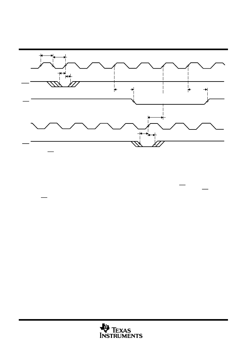
tsk2
(see Note C)
D
–
(m + 1) Words in FIFO
(see Notes A and B)
D
–
(m + 1)
Words in
FIFO
(see Notes
A and B)
WCLK
WEN
PAF
RCLK
REN
1
2
1
2
tCLKL
tENS
tENH
tPAFS
tPAES
tENS
tENH
D
–
m Words in FIFO
(see Notes A and B)
tCLKH
NOTES: A. m = PAF offset
B. D = maximum FIFO depth
In FWFT mode: If
×
18 input or
×
18 output bus width is selected, D = 8193 for the SN74V263, D = 16385 for the SN74V273,
D = 32769 for the SN74V283, and D = 65537 for the SN74V293. If both
×
9 input and
×
9 output bus widths are selected, D = 16385
for the SN74V263, D = 32769 for the SN74V273, D = 65537 for the SN74V283, and D = 131073 for the SN74V293.
In standard mode: If
×
18 input or
×
18 output bus width is selected, D = 8192 for the SN74V263, D = 16384 for the SN74V273,
D = 32768 for the SN74V283, and D = 65536 for the SN74V293. If both
×
9 Input and
×
9 output bus widths are selected, D = 16384
for the SN74V263, D = 32768 for the SN74V273, D = 65536 for the SN74V283, and D = 131072 for the SN74V293.
C. tsk2 is the minimum time between a rising RCLK edge and a rising WCLK edge to ensure that PAF goes high (after one WCLK
cycle + tPAFS). If the time between the rising edge of RCLK and the rising edge of WCLK is less than tsk2, the PAF deassertion
time may be delayed one additional WCLK cycle.
D. PAF is asserted and updated on the rising edge of WCLK only.
E. Select this mode by setting PFM high during master reset.
Figure 18. Synchronous Programmable Almost-Full Flag Timing (FWFT and Standard Modes)
相关PDF资料 |
PDF描述 |
|---|---|
| SN74V263-15GGM | 8192 】 18, 16384 】 18, 32768 】 18, 65536 】 18 3.3-V CMOS FIRST-IN, FIRST-OUT MEMORIES |
| SN74V263-7GGM | 8192 】 18, 16384 】 18, 32768 】 18, 65536 】 18 3.3-V CMOS FIRST-IN, FIRST-OUT MEMORIES |
| SN74V273-10GGM | 8192 】 18, 16384 】 18, 32768 】 18, 65536 】 18 3.3-V CMOS FIRST-IN, FIRST-OUT MEMORIES |
| SN74V273-15GGM | 8192 】 18, 16384 】 18, 32768 】 18, 65536 】 18 3.3-V CMOS FIRST-IN, FIRST-OUT MEMORIES |
| SN74V273-6GGM | 8192 】 18, 16384 】 18, 32768 】 18, 65536 】 18 3.3-V CMOS FIRST-IN, FIRST-OUT MEMORIES |
相关代理商/技术参数 |
参数描述 |
|---|---|
| SN74V263-10PZA | 功能描述:先进先出 8192 x 18 Synch 先进先出 Memory RoHS:否 制造商:IDT 电路数量: 数据总线宽度:18 bit 总线定向:Unidirectional 存储容量:4 Mbit 定时类型:Synchronous 组织:256 K x 18 最大时钟频率:100 MHz 访问时间:10 ns 电源电压-最大:3.6 V 电源电压-最小:6 V 最大工作电流:35 mA 最大工作温度:+ 85 C 封装 / 箱体:TQFP-80 封装: |
| SN74V263-15GGM | 功能描述:先进先出 8192 x 18 Synch 先进先出 Memory RoHS:否 制造商:IDT 电路数量: 数据总线宽度:18 bit 总线定向:Unidirectional 存储容量:4 Mbit 定时类型:Synchronous 组织:256 K x 18 最大时钟频率:100 MHz 访问时间:10 ns 电源电压-最大:3.6 V 电源电压-最小:6 V 最大工作电流:35 mA 最大工作温度:+ 85 C 封装 / 箱体:TQFP-80 封装: |
| SN74V263-15PZA | 功能描述:先进先出 8192 x 18 Synch 先进先出 Memory RoHS:否 制造商:IDT 电路数量: 数据总线宽度:18 bit 总线定向:Unidirectional 存储容量:4 Mbit 定时类型:Synchronous 组织:256 K x 18 最大时钟频率:100 MHz 访问时间:10 ns 电源电压-最大:3.6 V 电源电压-最小:6 V 最大工作电流:35 mA 最大工作温度:+ 85 C 封装 / 箱体:TQFP-80 封装: |
| SN74V263-6GGM | 功能描述:先进先出 8192 x 18 Synch 先进先出 Memory RoHS:否 制造商:IDT 电路数量: 数据总线宽度:18 bit 总线定向:Unidirectional 存储容量:4 Mbit 定时类型:Synchronous 组织:256 K x 18 最大时钟频率:100 MHz 访问时间:10 ns 电源电压-最大:3.6 V 电源电压-最小:6 V 最大工作电流:35 mA 最大工作温度:+ 85 C 封装 / 箱体:TQFP-80 封装: |
| SN74V263-6PZA | 功能描述:先进先出 8192 x 18 Synch 先进先出 Memory RoHS:否 制造商:IDT 电路数量: 数据总线宽度:18 bit 总线定向:Unidirectional 存储容量:4 Mbit 定时类型:Synchronous 组织:256 K x 18 最大时钟频率:100 MHz 访问时间:10 ns 电源电压-最大:3.6 V 电源电压-最小:6 V 最大工作电流:35 mA 最大工作温度:+ 85 C 封装 / 箱体:TQFP-80 封装: |
发布紧急采购,3分钟左右您将得到回复。