- 您现在的位置:买卖IC网 > PDF目录374873 > SN74V263-10GGM (Texas Instruments, Inc.) 8192 】 18, 16384 】 18, 32768 】 18, 65536 】 18 3.3-V CMOS FIRST-IN, FIRST-OUT MEMORIES PDF资料下载
参数资料
| 型号: | SN74V263-10GGM |
| 厂商: | Texas Instruments, Inc. |
| 英文描述: | 8192 】 18, 16384 】 18, 32768 】 18, 65536 】 18 3.3-V CMOS FIRST-IN, FIRST-OUT MEMORIES |
| 中文描述: | 8192】18,16384】18,32768】18,65536】18的3.3V的CMOS先入先出存储器 |
| 文件页数: | 46/52页 |
| 文件大小: | 762K |
| 代理商: | SN74V263-10GGM |
第1页第2页第3页第4页第5页第6页第7页第8页第9页第10页第11页第12页第13页第14页第15页第16页第17页第18页第19页第20页第21页第22页第23页第24页第25页第26页第27页第28页第29页第30页第31页第32页第33页第34页第35页第36页第37页第38页第39页第40页第41页第42页第43页第44页第45页当前第46页第47页第48页第49页第50页第51页第52页
SN74V263, SN74V273, SN74V283, SN74V293
8192
×
18, 16384
×
18, 32768
×
18, 65536
×
18
3.3-V CMOS FIRST-IN, FIRST-OUT MEMORIES
SCAS669D
–
JUNE 2001
–
REVISED FEBRUARY 2003
46
POST OFFICE BOX 655303
DALLAS, TEXAS 75265
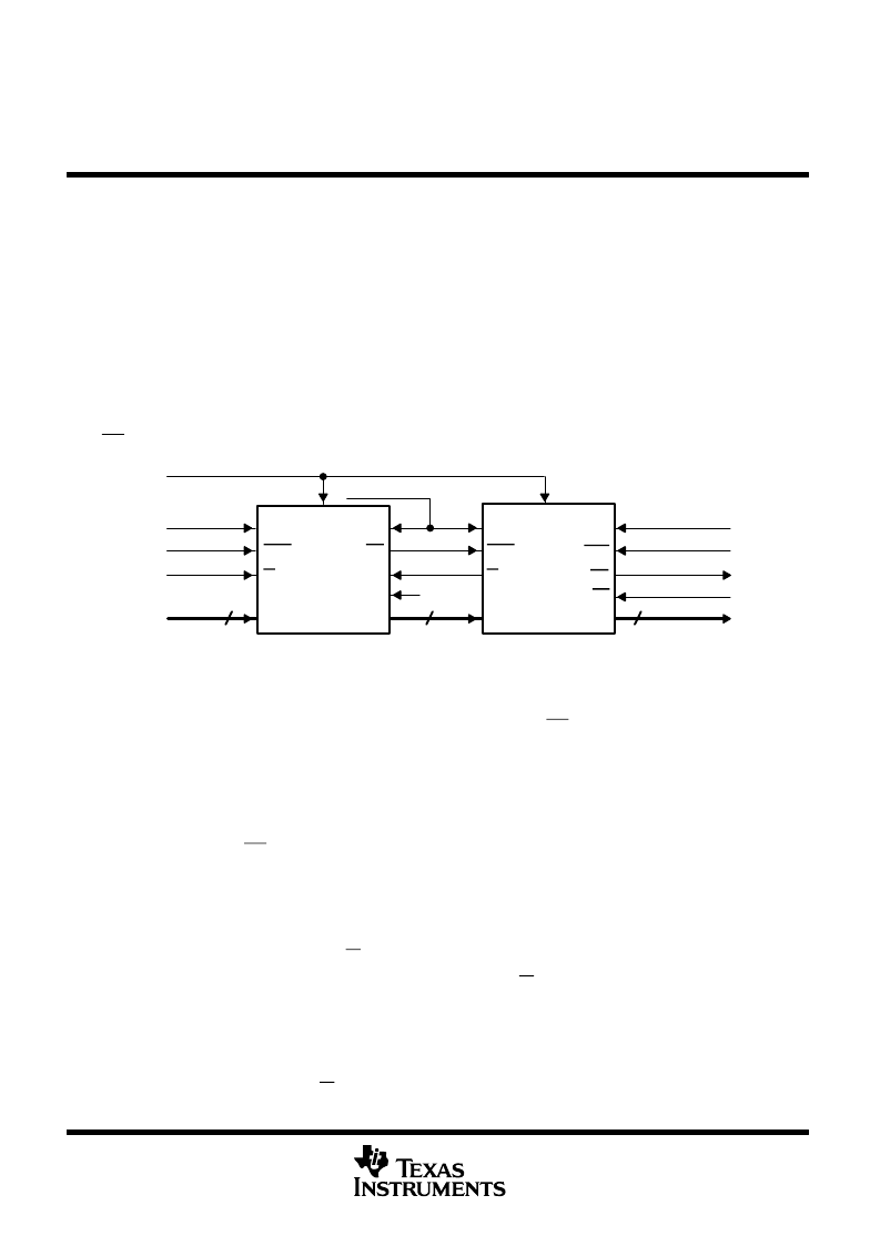
depth-expansion configuration (FWFT mode only)
The SN74V263 can be adapted easily to applications requiring depths greater than 8192 when the
×
18 input
or
×
18 output bus width is selected, 16384 for the SN74V273, 32768 for the SN74V283, and 65536 for the
SN74V293. When both
×
9 input and
×
9 output bus widths are selected, depths greater than 16384 can be
adapted for the SN74V263, 32768 for the SN74V273, 65536 for the SN74V283, and 131072 for the SN74V293.
In FWFT mode, the FIFOs can be connected in series (the data outputs of one FIFO connected to the data inputs
of the next), with no external logic necessary. The resulting configuration provides a total depth equivalent to
the sum of the dpths associated with each single FIFO. Figure 24 shows a depth expansion using two
SN74V263, SN74V273, SN74V283, and SN74V293 devices.
Care should be taken to select FWFT mode during master reset for all FIFOs in the depth-expansion
configuration. The first word written to an empty configuration passes from one FIFO to the next (ripple down)
until it finally appears at the outputs of the last FIFO in the chain. No read operation is necessary, but the RCLK
of each FIFO must be free running. Each time the data word appears at the outputs of one FIFO, that device
’
s
OR line goes low, enabling a write to the next FIFO in line.
REN
Data In
Write Enable
Write Clock
SN74V263
SN74V273
SN74V283
SN74V293
FWFT/SI
Transfer Clock
WCLK
WEN
IR
Dn
RCLK
OR
REN
OE
Qn
WCLK
WEN
IR
Dn
RCLK
OR
OE
Qn
Read Clock
Read Enable
Input Ready
Output Ready
Output Enable
Data Out
GND
n
n
n
SN74V263
SN74V273
SN74V283
SN74V293
FWFT/SI
FWFT/SI
Figure 24. Depth-Expansion Block Diagram
(For the
×
18 Input or
×
18 Output Bus Width: 16384
×
18, 32768
×
18, 65536
×
18, and 131072
×
18)
(For Both
×
9 Input and
×
9 Output Bus Width: 32768
×
9, 65536
×
9, 131072
×
9, and 262144
×
9)
For an empty expansion configuration, the amount of time it takes for OR of the last FIFO in the chain to go low
(i.e., valid data to appear on the last FIFO
’
s outputs) after a word has been written to the first FIFO is the sum
of the delays for each FIFO:
(N
–
1)
×
(4
×
transfer clock) + 3
×
T
RCLK
where N is the number of FIFOs in the expansion and T
RCLK
is the RCLK period. Note that extra cycles should
be added for the possibility that the t
sk1
specification is not met between WCLK and transfer clock, or RCLK and
transfer clock, for the OR flag.
The ripple-down delay is noticeable only for the first word written to an empty depth-expansion configuration.
There is no delay evident for subsequent words written to the configuration.
The first free location created by reading from a full-depth-expansion configuration bubbles up from the last
FIFO to the previous one until it finally moves into the first FIFO of the chain. Each time a free location is created
in one FIFO of the chain, that FIFO
’
s IR line goes low, enabling the preceding FIFO to write a word to fill it.
For a full-expansion configuration, the amount of time it takes for IR of the first FIFO in the chain to go low after
a word has been read from the last FIFO is the sum of the delays for each individual FIFO:
(N
–
1)
×
(3
×
transfer clock) + 2T
WCLK
where N is the number of FIFOs in the expansion and T
WCLK
is the WCLK period. Note that additional cycles
should be added for the possibility that the t
sk1
specification is not met between RCLK and transfer clock, or
WCLK and transfer clock, for the IR flag.
相关PDF资料 |
PDF描述 |
|---|---|
| SN74V263-15GGM | 8192 】 18, 16384 】 18, 32768 】 18, 65536 】 18 3.3-V CMOS FIRST-IN, FIRST-OUT MEMORIES |
| SN74V263-7GGM | 8192 】 18, 16384 】 18, 32768 】 18, 65536 】 18 3.3-V CMOS FIRST-IN, FIRST-OUT MEMORIES |
| SN74V273-10GGM | 8192 】 18, 16384 】 18, 32768 】 18, 65536 】 18 3.3-V CMOS FIRST-IN, FIRST-OUT MEMORIES |
| SN74V273-15GGM | 8192 】 18, 16384 】 18, 32768 】 18, 65536 】 18 3.3-V CMOS FIRST-IN, FIRST-OUT MEMORIES |
| SN74V273-6GGM | 8192 】 18, 16384 】 18, 32768 】 18, 65536 】 18 3.3-V CMOS FIRST-IN, FIRST-OUT MEMORIES |
相关代理商/技术参数 |
参数描述 |
|---|---|
| SN74V263-10PZA | 功能描述:先进先出 8192 x 18 Synch 先进先出 Memory RoHS:否 制造商:IDT 电路数量: 数据总线宽度:18 bit 总线定向:Unidirectional 存储容量:4 Mbit 定时类型:Synchronous 组织:256 K x 18 最大时钟频率:100 MHz 访问时间:10 ns 电源电压-最大:3.6 V 电源电压-最小:6 V 最大工作电流:35 mA 最大工作温度:+ 85 C 封装 / 箱体:TQFP-80 封装: |
| SN74V263-15GGM | 功能描述:先进先出 8192 x 18 Synch 先进先出 Memory RoHS:否 制造商:IDT 电路数量: 数据总线宽度:18 bit 总线定向:Unidirectional 存储容量:4 Mbit 定时类型:Synchronous 组织:256 K x 18 最大时钟频率:100 MHz 访问时间:10 ns 电源电压-最大:3.6 V 电源电压-最小:6 V 最大工作电流:35 mA 最大工作温度:+ 85 C 封装 / 箱体:TQFP-80 封装: |
| SN74V263-15PZA | 功能描述:先进先出 8192 x 18 Synch 先进先出 Memory RoHS:否 制造商:IDT 电路数量: 数据总线宽度:18 bit 总线定向:Unidirectional 存储容量:4 Mbit 定时类型:Synchronous 组织:256 K x 18 最大时钟频率:100 MHz 访问时间:10 ns 电源电压-最大:3.6 V 电源电压-最小:6 V 最大工作电流:35 mA 最大工作温度:+ 85 C 封装 / 箱体:TQFP-80 封装: |
| SN74V263-6GGM | 功能描述:先进先出 8192 x 18 Synch 先进先出 Memory RoHS:否 制造商:IDT 电路数量: 数据总线宽度:18 bit 总线定向:Unidirectional 存储容量:4 Mbit 定时类型:Synchronous 组织:256 K x 18 最大时钟频率:100 MHz 访问时间:10 ns 电源电压-最大:3.6 V 电源电压-最小:6 V 最大工作电流:35 mA 最大工作温度:+ 85 C 封装 / 箱体:TQFP-80 封装: |
| SN74V263-6PZA | 功能描述:先进先出 8192 x 18 Synch 先进先出 Memory RoHS:否 制造商:IDT 电路数量: 数据总线宽度:18 bit 总线定向:Unidirectional 存储容量:4 Mbit 定时类型:Synchronous 组织:256 K x 18 最大时钟频率:100 MHz 访问时间:10 ns 电源电压-最大:3.6 V 电源电压-最小:6 V 最大工作电流:35 mA 最大工作温度:+ 85 C 封装 / 箱体:TQFP-80 封装: |
发布紧急采购,3分钟左右您将得到回复。