- 您现在的位置:买卖IC网 > PDF目录374873 > SN74V263-10GGM (Texas Instruments, Inc.) 8192 】 18, 16384 】 18, 32768 】 18, 65536 】 18 3.3-V CMOS FIRST-IN, FIRST-OUT MEMORIES PDF资料下载
参数资料
| 型号: | SN74V263-10GGM |
| 厂商: | Texas Instruments, Inc. |
| 英文描述: | 8192 】 18, 16384 】 18, 32768 】 18, 65536 】 18 3.3-V CMOS FIRST-IN, FIRST-OUT MEMORIES |
| 中文描述: | 8192】18,16384】18,32768】18,65536】18的3.3V的CMOS先入先出存储器 |
| 文件页数: | 45/52页 |
| 文件大小: | 762K |
| 代理商: | SN74V263-10GGM |
第1页第2页第3页第4页第5页第6页第7页第8页第9页第10页第11页第12页第13页第14页第15页第16页第17页第18页第19页第20页第21页第22页第23页第24页第25页第26页第27页第28页第29页第30页第31页第32页第33页第34页第35页第36页第37页第38页第39页第40页第41页第42页第43页第44页当前第45页第46页第47页第48页第49页第50页第51页第52页
SN74V263, SN74V273, SN74V283, SN74V293
8192
×
18, 16384
×
18, 32768
×
18, 65536
×
18
3.3-V CMOS FIRST-IN, FIRST-OUT MEMORIES
SCAS669D
–
JUNE 2001
–
REVISED FEBRUARY 2003
45
POST OFFICE BOX 655303
DALLAS, TEXAS 75265
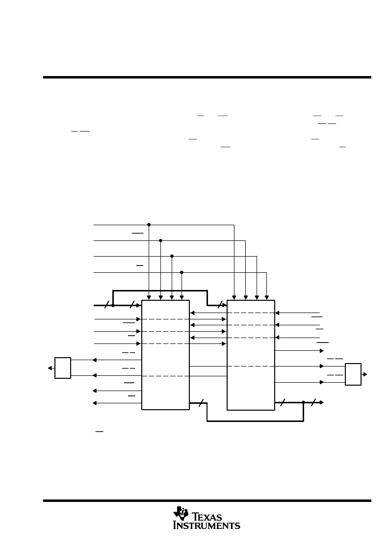
optional configurations
width expansion configuration
Word width can be increased by connecting the control signals of multiple devices. Status flags can be detected
from any one device. The exceptions are the the IR and OR functions in FWFT mode and EF and FF functions
in standard mode. Because of variations in skew between RCLK and WCLK, it is possible for EF/FF deassertion
and IR/OR assertion to vary by one cycle between FIFOs. In standard mode, such problems can be avoided
by creating composite flags, that is, ANDing EF of every FIFO and separately ANDing FF of every FIFO. In
FWFT mode, composite flags can be created by ORing OR of every FIFO and separately ORing IR of every
FIFO.
Figure 23 demonstrates a width expansion using two SN74V263, SN74V273, SN74V283, and SN74V293
devices. If
×
18 input or
×
18 output bus width is selected, D0
–
D17 from each device form a 36-bit-wide input bus,
and Q0
–
Q17 from each device form a 36-bit-wide output bus. If both
×
9 input and
×
9 output bus widths are
selected, D0
–
D8 from each device form an 18-bit-wide input bus, and Q0
–
Q8 from each device form an
18-bit-wide output bus. Any word width can be attained by adding additional SN74V263, SN74V273,
SN74V283, and SN74V293 devices.
Read Clock (RCLK)
Read Enable (REN)
Output Enable (OE)
Write Clock (WCLK)
Retransmit (RT)
Half-Full Flag (HF)
Write Enable (WEN)
Load (LD)
First-Word Fall-Through or Serial Input
(FWFT/SI)
Programmable
Almost-Full Flag (PAF)
Data In
Partial Reset (PRS)
Master Reset (MRS)
m + n
Full Flag/Input Ready 2
(FF/IR)
Full Flag/Input Ready 1
(FF/IR)
Empty Flag/Output Ready 2
(EF/OR)
D0
–
Dm
m
(Dm + 1)
–
Dn
n
Q0
–
Qm
m
n
(Qm + 1)
–
Qn
m + n
Data Out
SN74V263
SN74V273
SN74V283
SN74V293
SN74V263
SN74V273
SN74V283
SN74V293
Programmable (PAE)
Empty Flag/Output Ready 1
(EF/OR)
Gate
Gate
NOTES: A. Use an OR gate in FWFT mode and an AND gate in standard mode.
B. Do not connect any output control signals together directly.
C. FIFO 1 and FIFO 2 must be the same depth, but can be different word widths.
(see Note A)
(see Note A)
FIFO 1
FIFO 2
Figure 23. Width-Expansion Block Diagam
(For the
×
18 Input or
×
18 Output Bus Width: 8192
×
36, 16384
×
36, 32768
×
36, and 65536
×
36)
(For Both
×
9 Input and
×
9 Output Bus Widths: 16284
×
18, 32768
×
18, 65536
×
18, and 131072
×
18)
相关PDF资料 |
PDF描述 |
|---|---|
| SN74V263-15GGM | 8192 】 18, 16384 】 18, 32768 】 18, 65536 】 18 3.3-V CMOS FIRST-IN, FIRST-OUT MEMORIES |
| SN74V263-7GGM | 8192 】 18, 16384 】 18, 32768 】 18, 65536 】 18 3.3-V CMOS FIRST-IN, FIRST-OUT MEMORIES |
| SN74V273-10GGM | 8192 】 18, 16384 】 18, 32768 】 18, 65536 】 18 3.3-V CMOS FIRST-IN, FIRST-OUT MEMORIES |
| SN74V273-15GGM | 8192 】 18, 16384 】 18, 32768 】 18, 65536 】 18 3.3-V CMOS FIRST-IN, FIRST-OUT MEMORIES |
| SN74V273-6GGM | 8192 】 18, 16384 】 18, 32768 】 18, 65536 】 18 3.3-V CMOS FIRST-IN, FIRST-OUT MEMORIES |
相关代理商/技术参数 |
参数描述 |
|---|---|
| SN74V263-10PZA | 功能描述:先进先出 8192 x 18 Synch 先进先出 Memory RoHS:否 制造商:IDT 电路数量: 数据总线宽度:18 bit 总线定向:Unidirectional 存储容量:4 Mbit 定时类型:Synchronous 组织:256 K x 18 最大时钟频率:100 MHz 访问时间:10 ns 电源电压-最大:3.6 V 电源电压-最小:6 V 最大工作电流:35 mA 最大工作温度:+ 85 C 封装 / 箱体:TQFP-80 封装: |
| SN74V263-15GGM | 功能描述:先进先出 8192 x 18 Synch 先进先出 Memory RoHS:否 制造商:IDT 电路数量: 数据总线宽度:18 bit 总线定向:Unidirectional 存储容量:4 Mbit 定时类型:Synchronous 组织:256 K x 18 最大时钟频率:100 MHz 访问时间:10 ns 电源电压-最大:3.6 V 电源电压-最小:6 V 最大工作电流:35 mA 最大工作温度:+ 85 C 封装 / 箱体:TQFP-80 封装: |
| SN74V263-15PZA | 功能描述:先进先出 8192 x 18 Synch 先进先出 Memory RoHS:否 制造商:IDT 电路数量: 数据总线宽度:18 bit 总线定向:Unidirectional 存储容量:4 Mbit 定时类型:Synchronous 组织:256 K x 18 最大时钟频率:100 MHz 访问时间:10 ns 电源电压-最大:3.6 V 电源电压-最小:6 V 最大工作电流:35 mA 最大工作温度:+ 85 C 封装 / 箱体:TQFP-80 封装: |
| SN74V263-6GGM | 功能描述:先进先出 8192 x 18 Synch 先进先出 Memory RoHS:否 制造商:IDT 电路数量: 数据总线宽度:18 bit 总线定向:Unidirectional 存储容量:4 Mbit 定时类型:Synchronous 组织:256 K x 18 最大时钟频率:100 MHz 访问时间:10 ns 电源电压-最大:3.6 V 电源电压-最小:6 V 最大工作电流:35 mA 最大工作温度:+ 85 C 封装 / 箱体:TQFP-80 封装: |
| SN74V263-6PZA | 功能描述:先进先出 8192 x 18 Synch 先进先出 Memory RoHS:否 制造商:IDT 电路数量: 数据总线宽度:18 bit 总线定向:Unidirectional 存储容量:4 Mbit 定时类型:Synchronous 组织:256 K x 18 最大时钟频率:100 MHz 访问时间:10 ns 电源电压-最大:3.6 V 电源电压-最小:6 V 最大工作电流:35 mA 最大工作温度:+ 85 C 封装 / 箱体:TQFP-80 封装: |
发布紧急采购,3分钟左右您将得到回复。