- 您现在的位置:买卖IC网 > PDF目录98141 > SPAKXC16Z1VFV20 (MOTOROLA INC) 16-BIT, 20 MHz, MICROCONTROLLER, PQFP144 PDF资料下载
参数资料
| 型号: | SPAKXC16Z1VFV20 |
| 厂商: | MOTOROLA INC |
| 元件分类: | 微控制器/微处理器 |
| 英文描述: | 16-BIT, 20 MHz, MICROCONTROLLER, PQFP144 |
| 封装: | PLASTIC, SMT-144 |
| 文件页数: | 152/200页 |
| 文件大小: | 1383K |
| 代理商: | SPAKXC16Z1VFV20 |
第1页第2页第3页第4页第5页第6页第7页第8页第9页第10页第11页第12页第13页第14页第15页第16页第17页第18页第19页第20页第21页第22页第23页第24页第25页第26页第27页第28页第29页第30页第31页第32页第33页第34页第35页第36页第37页第38页第39页第40页第41页第42页第43页第44页第45页第46页第47页第48页第49页第50页第51页第52页第53页第54页第55页第56页第57页第58页第59页第60页第61页第62页第63页第64页第65页第66页第67页第68页第69页第70页第71页第72页第73页第74页第75页第76页第77页第78页第79页第80页第81页第82页第83页第84页第85页第86页第87页第88页第89页第90页第91页第92页第93页第94页第95页第96页第97页第98页第99页第100页第101页第102页第103页第104页第105页第106页第107页第108页第109页第110页第111页第112页第113页第114页第115页第116页第117页第118页第119页第120页第121页第122页第123页第124页第125页第126页第127页第128页第129页第130页第131页第132页第133页第134页第135页第136页第137页第138页第139页第140页第141页第142页第143页第144页第145页第146页第147页第148页第149页第150页第151页当前第152页第153页第154页第155页第156页第157页第158页第159页第160页第161页第162页第163页第164页第165页第166页第167页第168页第169页第170页第171页第172页第173页第174页第175页第176页第177页第178页第179页第180页第181页第182页第183页第184页第185页第186页第187页第188页第189页第190页第191页第192页第193页第194页第195页第196页第197页第198页第199页第200页
MC68HC16Z1
MOTOROLA
MC68HC16Z1TS/D
55
For example, if the MCU is executing an instruction that reads a long-word operand from a 16-bit port,
the MCU latches the 16 bits of valid data and then runs another bus cycle to obtain the other 16 bits.
The operation for an 8-bit port is similar, but requires four read cycles. The addressed device uses the
DSACK0 and DSACK1 signals to indicate the port width. For instance, a 16-bit device always returns
DSACK0 = 1 and DSACK1 = 0 for a 16-bit port, regardless of whether the bus cycle is a byte or word
operation.
Dynamic bus sizing requires that the portion of the data bus used for a transfer to or from a particular
port size be fixed. A 16-bit port must reside on data bus bits [15:0] and an 8-bit port must reside on data
bus bits [15:8]. This minimizes the number of bus cycles needed to transfer data and ensures that the
MCU transfers valid data.
The MCU always attempts to transfer the maximum amount of data on all bus cycles. For a word oper-
ation, it is assumed that the port is 16 bits wide when the bus cycle begins. Operand bytes are desig-
nated as shown in the following figure. OP0 is the most significant byte of a long-word operand, and
OP3 is the least significant byte. The two bytes of a word-length operand are OP0 (most significant) and
OP1. The single byte of a byte-length operand is OP0.
Figure 11 Operand Byte Order
3.5.10 Operand Alignment
The data multiplexer establishes the necessary connections for different combinations of address and
data sizes. The multiplexer takes the two bytes of the 16-bit bus and routes them to their required po-
sitions. Positioning of bytes is determined by the size and address outputs. SIZ1 and SIZ0 indicate the
remaining number of bytes to be transferred during the current bus cycle. The number of bytes trans-
ferred is equal to or less than the size indicated by SIZ1 and SIZ0, depending on port width.
ADDR0 also affects the operation of the data multiplexer. During an operand transfer, ADDR[23:1] in-
dicate the word base address of the portion of the operand to be accessed, and ADDR0 indicates the
byte offset from the base. Bear in mind the fact that ADDR[23:20] follow the state of ADDR19 in the
MC68HC16Z1.
3.5.11 Misaligned Operands
CPU16 processor architecture uses a basic operand size of 16 bits. An operand is misaligned when it
overlaps a word boundary. This is determined by the value of ADDR0. When ADDR0 = 0 (an even ad-
dress), the address is on a word and byte boundary. When ADDR0 = 1 (an odd address), the address
is on a byte boundary only. A byte operand is aligned at any address; a word or long-word operand is
misaligned at an odd address.
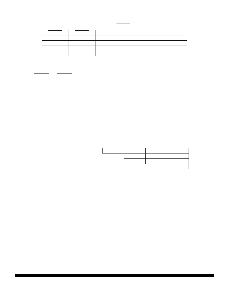
Table 13 Effect of DSACK Signals
DSACK1
DSACK0
Result
1
Insert Wait States in Current Bus Cycle
1
0
Complete Cycle — Data Bus Port Size is 8 Bits
0
1
Complete Cycle — Data Bus Port Size is 16 Bits
0
Reserved
Operand
Byte Order
31
24
23
16
15
8
7
0
Long Word
OP0
OP1
OP2
OP3
Three Byte
OP0
OP1
OP2
Word
OP0
OP1
Byte
OP0
相关PDF资料 |
PDF描述 |
|---|---|
| SPAKXCF333CFT20 | 32-BIT, FLASH, 20 MHz, MICROCONTROLLER, PQFP16 |
| SPAKXCF333MFT20 | 32-BIT, FLASH, 20 MHz, MICROCONTROLLER, PQFP16 |
| SPAKXCF333VFT20 | 32-BIT, FLASH, 20 MHz, MICROCONTROLLER, PQFP16 |
| SPC3010F | 24 Mbps, FIXED DISK CONTROLLER, PQFP100 |
| SPC560B50L5C5E0R | 32-BIT, FLASH, 64 MHz, MICROCONTROLLER, PQFP144 |
相关代理商/技术参数 |
参数描述 |
|---|---|
| SPAKXC301GC100D | 制造商:Motorola Inc 功能描述: |
| SPAKXC301PW100D | 制造商:Motorola Inc 功能描述: |
| SPAKXC309AG100A | 功能描述:数字信号处理器和控制器 - DSP, DSC 24 BIT DSP PBFREE RoHS:否 制造商:Microchip Technology 核心:dsPIC 数据总线宽度:16 bit 程序存储器大小:16 KB 数据 RAM 大小:2 KB 最大时钟频率:40 MHz 可编程输入/输出端数量:35 定时器数量:3 设备每秒兆指令数:50 MIPs 工作电源电压:3.3 V 最大工作温度:+ 85 C 封装 / 箱体:TQFP-44 安装风格:SMD/SMT |
| SPAKXC309GC100A | 制造商:Motorola 功能描述:MOTOROLA |
| SPAKXC309VF100A | 功能描述:IC DSP 24BIT 100MHZ 196-MAPBGA RoHS:否 类别:集成电路 (IC) >> 嵌入式 - DSP(数字式信号处理器) 系列:DSP563xx 标准包装:40 系列:TMS320DM64x, DaVinci™ 类型:定点 接口:I²C,McASP,McBSP 时钟速率:400MHz 非易失内存:外部 芯片上RAM:160kB 电压 - 输入/输出:3.30V 电压 - 核心:1.20V 工作温度:0°C ~ 90°C 安装类型:表面贴装 封装/外壳:548-BBGA,FCBGA 供应商设备封装:548-FCBGA(27x27) 包装:托盘 配用:TMDSDMK642-0E-ND - DEVELPER KIT W/NTSC CAMERA296-23038-ND - DSP STARTER KIT FOR TMS320C6416296-23059-ND - FLASHBURN PORTING KIT296-23058-ND - EVAL MODULE FOR DM642TMDSDMK642-ND - DEVELOPER KIT W/NTSC CAMERA |
发布紧急采购,3分钟左右您将得到回复。