- 您现在的位置:买卖IC网 > PDF目录98141 > SPAKXC16Z1VFV20 (MOTOROLA INC) 16-BIT, 20 MHz, MICROCONTROLLER, PQFP144 PDF资料下载
参数资料
| 型号: | SPAKXC16Z1VFV20 |
| 厂商: | MOTOROLA INC |
| 元件分类: | 微控制器/微处理器 |
| 英文描述: | 16-BIT, 20 MHz, MICROCONTROLLER, PQFP144 |
| 封装: | PLASTIC, SMT-144 |
| 文件页数: | 59/200页 |
| 文件大小: | 1383K |
| 代理商: | SPAKXC16Z1VFV20 |
第1页第2页第3页第4页第5页第6页第7页第8页第9页第10页第11页第12页第13页第14页第15页第16页第17页第18页第19页第20页第21页第22页第23页第24页第25页第26页第27页第28页第29页第30页第31页第32页第33页第34页第35页第36页第37页第38页第39页第40页第41页第42页第43页第44页第45页第46页第47页第48页第49页第50页第51页第52页第53页第54页第55页第56页第57页第58页当前第59页第60页第61页第62页第63页第64页第65页第66页第67页第68页第69页第70页第71页第72页第73页第74页第75页第76页第77页第78页第79页第80页第81页第82页第83页第84页第85页第86页第87页第88页第89页第90页第91页第92页第93页第94页第95页第96页第97页第98页第99页第100页第101页第102页第103页第104页第105页第106页第107页第108页第109页第110页第111页第112页第113页第114页第115页第116页第117页第118页第119页第120页第121页第122页第123页第124页第125页第126页第127页第128页第129页第130页第131页第132页第133页第134页第135页第136页第137页第138页第139页第140页第141页第142页第143页第144页第145页第146页第147页第148页第149页第150页第151页第152页第153页第154页第155页第156页第157页第158页第159页第160页第161页第162页第163页第164页第165页第166页第167页第168页第169页第170页第171页第172页第173页第174页第175页第176页第177页第178页第179页第180页第181页第182页第183页第184页第185页第186页第187页第188页第189页第190页第191页第192页第193页第194页第195页第196页第197页第198页第199页第200页
M68HC16ZEC20/D
MOTOROLA
7
NOTES:
1. Applies to:
Port ADA[7:0] — AN[7:0]
Port E[7:4] — SIZ[1:0], AS, DS
Port F[7:0] — IRQ[7:1], MODCLK
Port GP[7:0] — IC4/OC5/OC1, IC[3:1], OC[4:1]/OC1
Port QS[7:0] — TXD, PCS[3:1], PCS0/SS, SCK, MOSI, MISO
BKPT/DSCLK, DSI/IPIPE1, PAI, PCLK, RESET, RXD, TSC
EXTAL (when PLL enabled)
2. This parameter is periodically sampled rather than 100% tested.
3. Applies to all input-only pins except ADC pins.
4. Applies to all input/output and output pins
5. Does not apply to HALT and RESET because they are open drain pins. Does not apply to Port QS[7:0] (TXD,
PCS[3:1], PCS0/SS, SCK, MOSI, MISO) in wired-OR mode.
6. Applies to Group 1, 2, 4 input/output and all output pins
7. Applies to Group 1, 2, 3, 4 input/output pins, BG/CS, CLKOUT, CSBOOT, FREEZE/QUOT, and IPIPE0
8. Applies to DATA[15:0]
9. Use of an active pulldown device is recommended.
10. Total operating current is the sum of the appropriate IDD, IDDSYN, and ISB values, plus IDDA. IDD values in-
clude supply currents for device modules powered by VDDE and VDDI pins.
11. Current measured at maximum system clock frequency, all modules active.
12. The base configuration of the MC68HC16Z1 requires a 32.768 kHz crystal reference, and the base configu-
ration of the M68HC16Z2 requires a 4.194 MHz crystal reference. Both devices can be ordered with either
crystal reference as a mask option.
13. The SRAM module will not switch into standby mode as long as VSB does not exceed VDD by more than
0.5 volts. The SRAM array cannot be accessed while the module is in standby mode.
14. When VSB is more than 0.3 V greater than VDD, current flows between the VSTBY and VDD pins, which
causes standby current to increase toward the maximum transient condition specification. System noise on
the VDD and VSTBY pin can contribute to this condition.
15. Power dissipation measured at specified system clock frequency, all modules active. Power dissipation can
be calculated using the expression:
PD = Maximum VDD (IDD + IDDSYN + ISB) + Maximum VDDA (IDDA)
IDD includes supply currents for all device modules powered by VDDE and VDDI pins.
16. Input-Only Pins: EXTAL, TSC, BKPT/DSCLK, PAI, PCLK, RXD
Output-Only Pins: CSBOOT, BG/CS1, CLKOUT, FREEZE/QUOT, DS0/IPIPE0, PWMA, PWMB
Input/Output Pins:
Group 1: Port GP[7:0] — IC4/OC5/OC1, IC[3:1], OC[4:1]/OC1
DATA[15:0], DSI/IPIPE1
Group 2: Port C[6:0] — ADDR[22:19]/CS[9:6], FC[2:0]/CS[5:3]
Port E[7:0] — SIZ[1:0], AS, DS, AVEC, DSACK[1:0]
Port F[7:0] — IRQ[7:1], MODCLK
Port QS[7:3] — TXD, PCS[3:1], PCS0/SS, ADDR23/CS10/ECLK
ADDR[18:0], R/W, BERR, BR/CS0, BGACK/CS2
Group 3: HALT, RESET
Group 4: MISO, MOSI, SCK
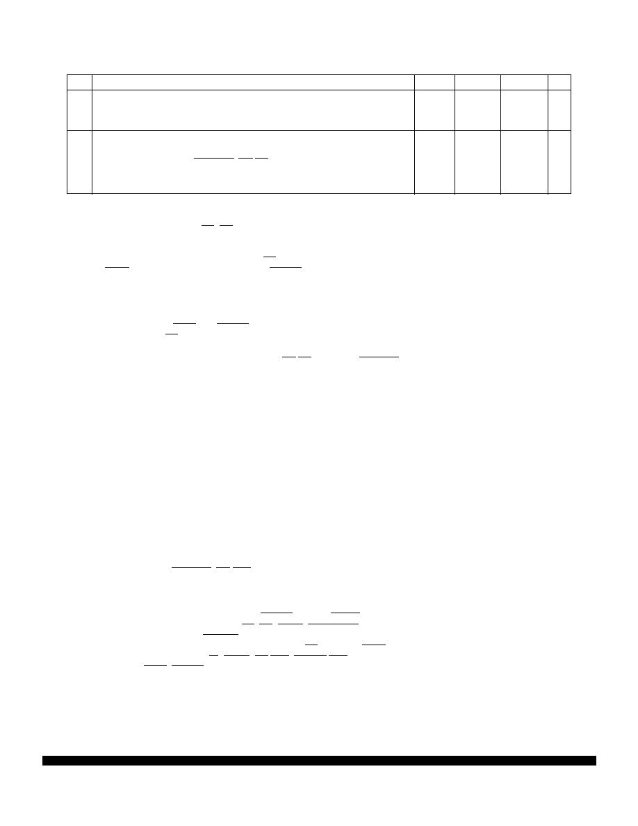
18
Input Capacitance3,16
All input-only pins except ADC pins
All input/output pins
Cin
—
10
20
pF
19
Load Capacitance16
Group 1 I/O Pins, CLKOUT, FREEZE/QUOT, IPIPE0
Group 2 I/O Pins and CSBOOT, BG/CS
Group 3 I/O Pins
Group 4 I/O Pins
CL
—
90
100
130
200
pF
Table A–5 DC Characteristics (Continued)
(V
DD
and V
DDSYN
= 5.0 Vdc
± 5%, V
SS
= 0 Vdc, T
A
= T
L
to T
H)
Num
Characteristic
Symbol
Min
Max
Unit
相关PDF资料 |
PDF描述 |
|---|---|
| SPAKXCF333CFT20 | 32-BIT, FLASH, 20 MHz, MICROCONTROLLER, PQFP16 |
| SPAKXCF333MFT20 | 32-BIT, FLASH, 20 MHz, MICROCONTROLLER, PQFP16 |
| SPAKXCF333VFT20 | 32-BIT, FLASH, 20 MHz, MICROCONTROLLER, PQFP16 |
| SPC3010F | 24 Mbps, FIXED DISK CONTROLLER, PQFP100 |
| SPC560B50L5C5E0R | 32-BIT, FLASH, 64 MHz, MICROCONTROLLER, PQFP144 |
相关代理商/技术参数 |
参数描述 |
|---|---|
| SPAKXC301GC100D | 制造商:Motorola Inc 功能描述: |
| SPAKXC301PW100D | 制造商:Motorola Inc 功能描述: |
| SPAKXC309AG100A | 功能描述:数字信号处理器和控制器 - DSP, DSC 24 BIT DSP PBFREE RoHS:否 制造商:Microchip Technology 核心:dsPIC 数据总线宽度:16 bit 程序存储器大小:16 KB 数据 RAM 大小:2 KB 最大时钟频率:40 MHz 可编程输入/输出端数量:35 定时器数量:3 设备每秒兆指令数:50 MIPs 工作电源电压:3.3 V 最大工作温度:+ 85 C 封装 / 箱体:TQFP-44 安装风格:SMD/SMT |
| SPAKXC309GC100A | 制造商:Motorola 功能描述:MOTOROLA |
| SPAKXC309VF100A | 功能描述:IC DSP 24BIT 100MHZ 196-MAPBGA RoHS:否 类别:集成电路 (IC) >> 嵌入式 - DSP(数字式信号处理器) 系列:DSP563xx 标准包装:40 系列:TMS320DM64x, DaVinci™ 类型:定点 接口:I²C,McASP,McBSP 时钟速率:400MHz 非易失内存:外部 芯片上RAM:160kB 电压 - 输入/输出:3.30V 电压 - 核心:1.20V 工作温度:0°C ~ 90°C 安装类型:表面贴装 封装/外壳:548-BBGA,FCBGA 供应商设备封装:548-FCBGA(27x27) 包装:托盘 配用:TMDSDMK642-0E-ND - DEVELPER KIT W/NTSC CAMERA296-23038-ND - DSP STARTER KIT FOR TMS320C6416296-23059-ND - FLASHBURN PORTING KIT296-23058-ND - EVAL MODULE FOR DM642TMDSDMK642-ND - DEVELOPER KIT W/NTSC CAMERA |
发布紧急采购,3分钟左右您将得到回复。