- 您现在的位置:买卖IC网 > PDF目录98141 > SPAKXC16Z1VFV20 (MOTOROLA INC) 16-BIT, 20 MHz, MICROCONTROLLER, PQFP144 PDF资料下载
参数资料
| 型号: | SPAKXC16Z1VFV20 |
| 厂商: | MOTOROLA INC |
| 元件分类: | 微控制器/微处理器 |
| 英文描述: | 16-BIT, 20 MHz, MICROCONTROLLER, PQFP144 |
| 封装: | PLASTIC, SMT-144 |
| 文件页数: | 3/200页 |
| 文件大小: | 1383K |
| 代理商: | SPAKXC16Z1VFV20 |
第1页第2页当前第3页第4页第5页第6页第7页第8页第9页第10页第11页第12页第13页第14页第15页第16页第17页第18页第19页第20页第21页第22页第23页第24页第25页第26页第27页第28页第29页第30页第31页第32页第33页第34页第35页第36页第37页第38页第39页第40页第41页第42页第43页第44页第45页第46页第47页第48页第49页第50页第51页第52页第53页第54页第55页第56页第57页第58页第59页第60页第61页第62页第63页第64页第65页第66页第67页第68页第69页第70页第71页第72页第73页第74页第75页第76页第77页第78页第79页第80页第81页第82页第83页第84页第85页第86页第87页第88页第89页第90页第91页第92页第93页第94页第95页第96页第97页第98页第99页第100页第101页第102页第103页第104页第105页第106页第107页第108页第109页第110页第111页第112页第113页第114页第115页第116页第117页第118页第119页第120页第121页第122页第123页第124页第125页第126页第127页第128页第129页第130页第131页第132页第133页第134页第135页第136页第137页第138页第139页第140页第141页第142页第143页第144页第145页第146页第147页第148页第149页第150页第151页第152页第153页第154页第155页第156页第157页第158页第159页第160页第161页第162页第163页第164页第165页第166页第167页第168页第169页第170页第171页第172页第173页第174页第175页第176页第177页第178页第179页第180页第181页第182页第183页第184页第185页第186页第187页第188页第189页第190页第191页第192页第193页第194页第195页第196页第197页第198页第199页第200页
MOTOROLA
MC68HC16Z1
100
MC68HC16Z1TS/D
RASP[1:0] — RAM Array Space Field
This field limits access to the SRAM array in microcontrollers that support separate user and supervisor
operating modes. Because the CPU16 operates in supervisor mode only, RASP1 has no effect.
RAMTST — RAM Test Register
$YFFB02
RAMTST is for factory test only. Reads of this register return zeros and writes have no effect.
*ADDR[23:20] is at the same logic level as ADDR19 during internal CPU master operation. ADDR[23:20] must
match ADDR19 for the chip select to be active.
RAMBAH and RAMBAL specify an SRAM base address in the system memory map. They can only be
written while the SRAM is in low-power mode (RAMMCR STOP = 1, the default out of reset) and the
base address lock is disabled (RAMMCR RLCK = 0, the default out of reset). This prevents accidental
remapping of the array. Because the CPU16 drives ADDR[23:20] with the value of ADDR19, the value
in the ADDR[23:20] fields must match the value in the ADDR19 field for the array to be accessible.
6.3 SRAM Operation
There are five operating modes.
The RAM module is in normal mode when powered by VDD. The array can be accessed by byte, word,
or long word. A byte or aligned word (high-order byte is at an even address) access only takes one bus
cycle or two system clocks. A long word or misaligned word access requires two bus cycles.
Standby mode is intended to preserve RAM contents when VDD is removed. SRAM contents are main-
tained by a power source connected to the VSTBY pin. The standby voltage is referred to as VSB. Cir-
cuitry within the SRAM module switches to the higher of VDD or VSB with no loss of data. When SRAM
is powered from the VSTBY pin, access to the array is not guaranteed. If standby operation is not desired,
connect the VSTBY pin to VSS.
Reset mode allows the CPU to complete the current bus cycle before resetting. When a synchronous
reset occurs while a byte or word SRAM access is in progress, the access will be completed. If reset
occurs during the first word access of a long-word operation, only the first word access will be complet-
ed. If reset occurs during the second word access of a long word operation, the entire access will be
completed. Data being read from or written to the RAM may be corrupted by asynchronous reset.
Test mode is used for factory testing of the RAM array.
Writing the STOP bit of RAMMCR causes the SRAM module to enter stop mode. The RAM array is dis-
abled which, if necessary, allows external logic to decode SRAM addresses but all data is retained. If
VDD falls below VSB, internal circuitry switches to VSB, as in standby mode. Exit the stop mode by clear-
ing the STOP bit.
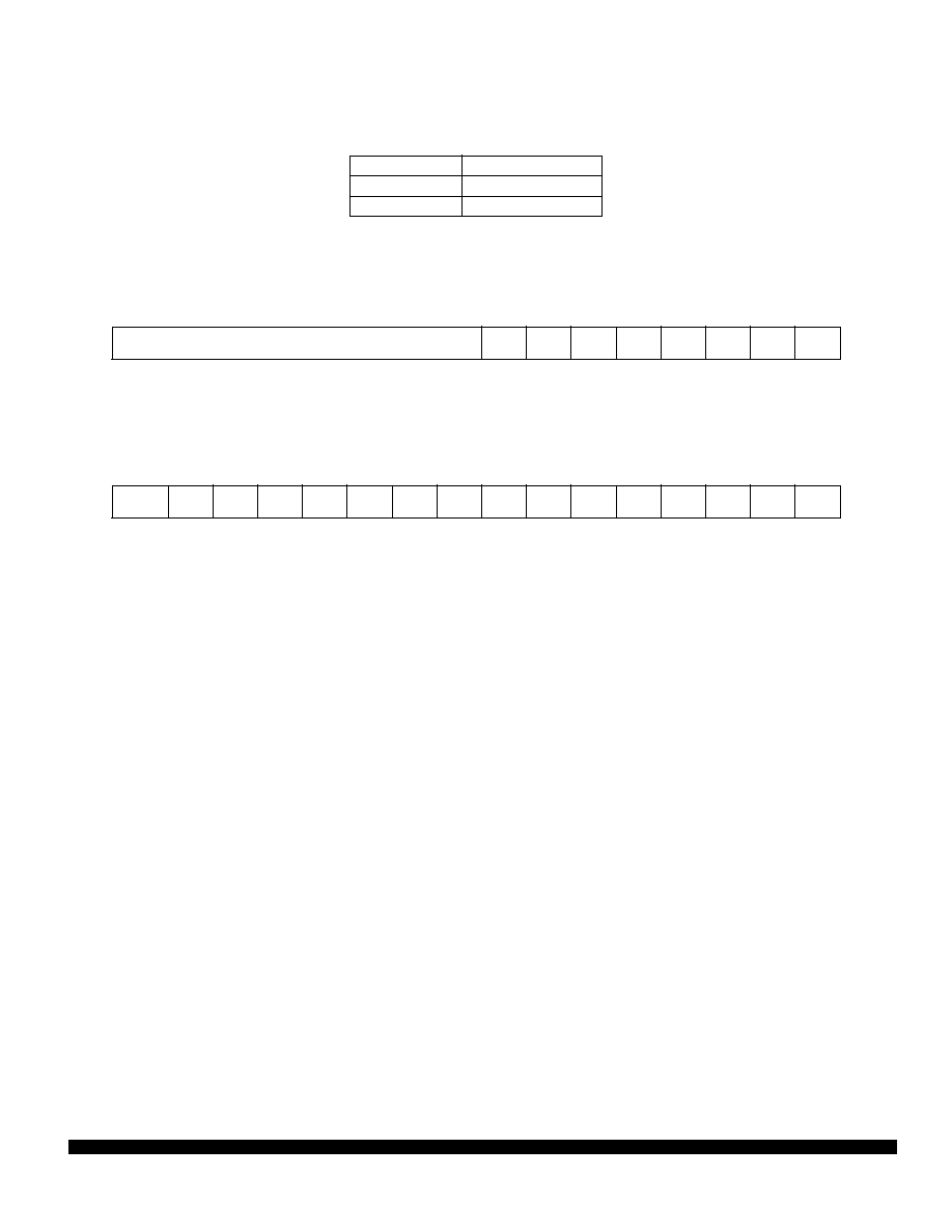
RASP
Space
X0
Program and Data
X1
Program
RAMBAH — Array Base Address Register High
$YFFB04
15
14
13
12
11
10
9
8
7
6
5
4
3
2
1
0
NOT USED
ADDR
23*
ADDR
22*
ADDR
21*
ADDR
20*
ADDR
19
ADDR
18
ADDR
17
ADDR
16
RESET:
0
RAMBAL — Array Base Address Register Low
$YFFB06
15
14
13
12
11
10
9
8
7
6
5
4
3
2
1
0
ADDR
15
ADDR
14
ADDR
13
ADDR
12
ADDR
11
ADDR
10
ADDR
9
ADDR
8
ADDR
7
ADDR
6
ADDR
5
ADDR
4
ADDR
3
ADDR
2
ADDR
1
ADDR
0
RESET:
0
相关PDF资料 |
PDF描述 |
|---|---|
| SPAKXCF333CFT20 | 32-BIT, FLASH, 20 MHz, MICROCONTROLLER, PQFP16 |
| SPAKXCF333MFT20 | 32-BIT, FLASH, 20 MHz, MICROCONTROLLER, PQFP16 |
| SPAKXCF333VFT20 | 32-BIT, FLASH, 20 MHz, MICROCONTROLLER, PQFP16 |
| SPC3010F | 24 Mbps, FIXED DISK CONTROLLER, PQFP100 |
| SPC560B50L5C5E0R | 32-BIT, FLASH, 64 MHz, MICROCONTROLLER, PQFP144 |
相关代理商/技术参数 |
参数描述 |
|---|---|
| SPAKXC301GC100D | 制造商:Motorola Inc 功能描述: |
| SPAKXC301PW100D | 制造商:Motorola Inc 功能描述: |
| SPAKXC309AG100A | 功能描述:数字信号处理器和控制器 - DSP, DSC 24 BIT DSP PBFREE RoHS:否 制造商:Microchip Technology 核心:dsPIC 数据总线宽度:16 bit 程序存储器大小:16 KB 数据 RAM 大小:2 KB 最大时钟频率:40 MHz 可编程输入/输出端数量:35 定时器数量:3 设备每秒兆指令数:50 MIPs 工作电源电压:3.3 V 最大工作温度:+ 85 C 封装 / 箱体:TQFP-44 安装风格:SMD/SMT |
| SPAKXC309GC100A | 制造商:Motorola 功能描述:MOTOROLA |
| SPAKXC309VF100A | 功能描述:IC DSP 24BIT 100MHZ 196-MAPBGA RoHS:否 类别:集成电路 (IC) >> 嵌入式 - DSP(数字式信号处理器) 系列:DSP563xx 标准包装:40 系列:TMS320DM64x, DaVinci™ 类型:定点 接口:I²C,McASP,McBSP 时钟速率:400MHz 非易失内存:外部 芯片上RAM:160kB 电压 - 输入/输出:3.30V 电压 - 核心:1.20V 工作温度:0°C ~ 90°C 安装类型:表面贴装 封装/外壳:548-BBGA,FCBGA 供应商设备封装:548-FCBGA(27x27) 包装:托盘 配用:TMDSDMK642-0E-ND - DEVELPER KIT W/NTSC CAMERA296-23038-ND - DSP STARTER KIT FOR TMS320C6416296-23059-ND - FLASHBURN PORTING KIT296-23058-ND - EVAL MODULE FOR DM642TMDSDMK642-ND - DEVELOPER KIT W/NTSC CAMERA |
发布紧急采购,3分钟左右您将得到回复。