- 您现在的位置:买卖IC网 > PDF目录98141 > SPAKXC16Z1VFV20 (MOTOROLA INC) 16-BIT, 20 MHz, MICROCONTROLLER, PQFP144 PDF资料下载
参数资料
| 型号: | SPAKXC16Z1VFV20 |
| 厂商: | MOTOROLA INC |
| 元件分类: | 微控制器/微处理器 |
| 英文描述: | 16-BIT, 20 MHz, MICROCONTROLLER, PQFP144 |
| 封装: | PLASTIC, SMT-144 |
| 文件页数: | 200/200页 |
| 文件大小: | 1383K |
| 代理商: | SPAKXC16Z1VFV20 |
第1页第2页第3页第4页第5页第6页第7页第8页第9页第10页第11页第12页第13页第14页第15页第16页第17页第18页第19页第20页第21页第22页第23页第24页第25页第26页第27页第28页第29页第30页第31页第32页第33页第34页第35页第36页第37页第38页第39页第40页第41页第42页第43页第44页第45页第46页第47页第48页第49页第50页第51页第52页第53页第54页第55页第56页第57页第58页第59页第60页第61页第62页第63页第64页第65页第66页第67页第68页第69页第70页第71页第72页第73页第74页第75页第76页第77页第78页第79页第80页第81页第82页第83页第84页第85页第86页第87页第88页第89页第90页第91页第92页第93页第94页第95页第96页第97页第98页第99页第100页第101页第102页第103页第104页第105页第106页第107页第108页第109页第110页第111页第112页第113页第114页第115页第116页第117页第118页第119页第120页第121页第122页第123页第124页第125页第126页第127页第128页第129页第130页第131页第132页第133页第134页第135页第136页第137页第138页第139页第140页第141页第142页第143页第144页第145页第146页第147页第148页第149页第150页第151页第152页第153页第154页第155页第156页第157页第158页第159页第160页第161页第162页第163页第164页第165页第166页第167页第168页第169页第170页第171页第172页第173页第174页第175页第176页第177页第178页第179页第180页第181页第182页第183页第184页第185页第186页第187页第188页第189页第190页第191页第192页第193页第194页第195页第196页第197页第198页第199页当前第200页
MC68HC16Z1
MOTOROLA
MC68HC16Z1TS/D
99
6 Standby RAM Module
This module contains a one Kbyte array of fast (two bus cycle) static RAM, which is especially useful
for system stacks and variable storage. SRAM can be mapped to any one Kbyte boundary in the ad-
dress map, but must not overlap the module control registers (overlap makes the registers inaccessi-
ble). Data can be read/written in bytes, words or long words. SRAM is powered by VDD in normal
operation. During power-down, SRAM contents are maintained by power from the VSTBY input. Power
switching between sources is automatic. An address map of the SRAM control registers follows.
Y = M111, where M is the logic state of the modmap (MM) bit in the SIMCR
6.1 SRAM Register Block
There are four SRAM control registers: the RAM module configuration register (RAMMCR), the RAM
test register (RAMTST), and the RAM array base address registers (RAMBAH/RAMBAL).
There is an 8-byte minimum register block size for the module. Unimplemented register addresses are
read as zeros. Writes have no effect.
6.2 SRAM Registers
The CPU16 in the MC68HC16Z1 operates only in supervisory mode. Access to the SRAM array is con-
trolled by the RASP field in RAMMCR. SRAM responds to both program and data space accesses
based on the value in the RASP field in RAMMCR. This allows code to be executed from RAM, and
permits the use of program counter relative addressing mode for operand fetches from the array.
Use RAMMCR to determine whether the RAM is in STOP mode or normal mode. It can also determine
in which space the array resides, and controls access to the base array registers. Reads of unimple-
mented bits always return zeros. Writes do not affect unimplemented bits.
STOP — Stop Control
0 = RAM array operates normally.
1 = RAM array enters low-power stop mode.
This bit controls whether the RAM array is in stop mode or normal operation. Reset state is one, leaving
the array configured for LPSTOP operation. In stop mode, the array retains its contents, but cannot be
read or written by the CPU. Because the CPU16 operates in supervisor mode, this bit can be read or
written at any time.
RLCK — RAM Base Address Lock
0 = SRAM base address registers are writable from IMB
1 = SRAM base address registers are locked
RLCK defaults to zero on reset. It can be written to one once.
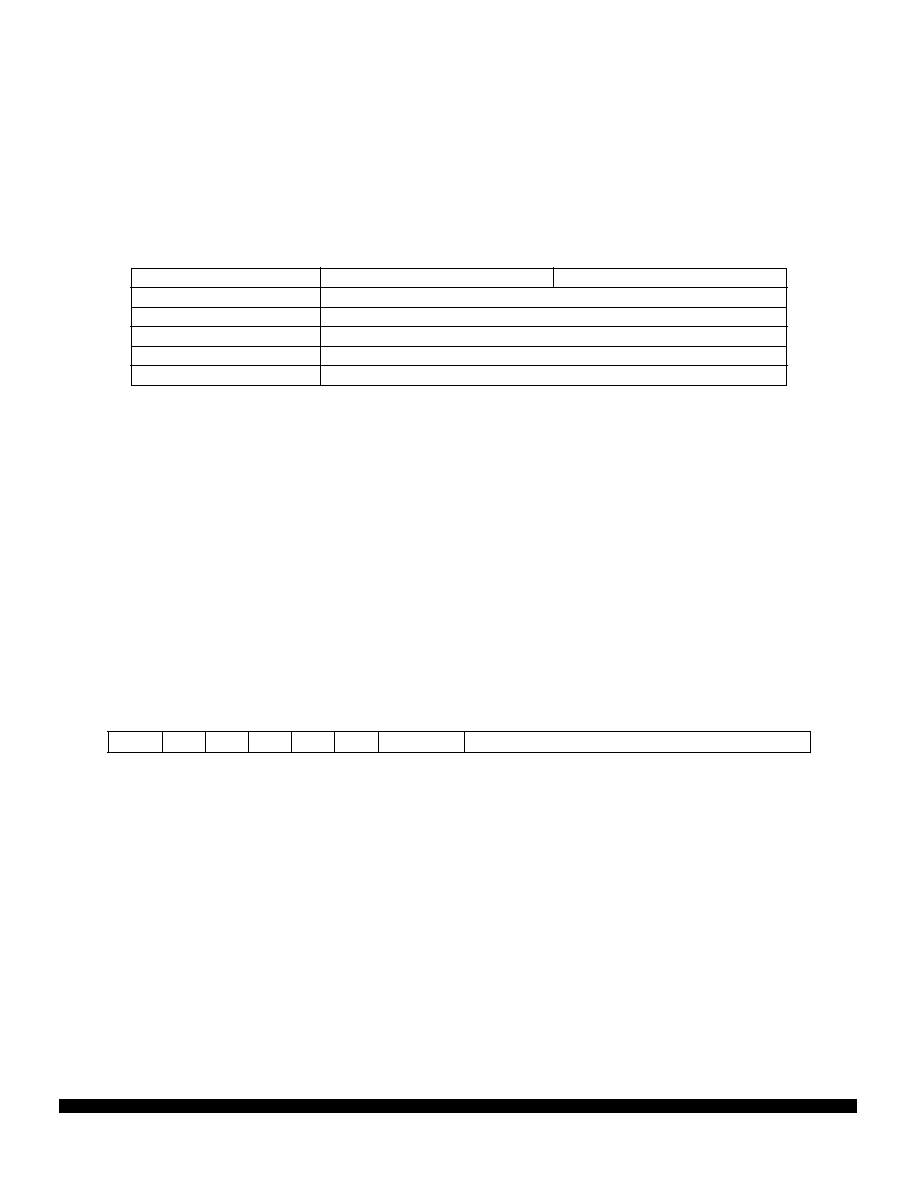
Table 19 SRAM Address Map
Address
15
8
7
0
$YFFB00
RAM MODULE CONFIGURATION REGISTER (RAMMCR)
$YFFB02
RAM TEST REGISTER (RAMTST)
$YFFB04
RAM ARRAY BASE ADDRESS REGISTER HIGH (RAMBAH)
$YFFB06
RAM ARRAY BASE ADDRESS REGISTER LOW (RAMBAL)
$YFFB08
RESERVED
RAMMCR — RAM Module Configuration Register
$YFFB00
15
11
9
8
7
6
5
4
3
2
1
0
STOP
0
RLCK
0
RASP
NOT USED
RESET:
1
0
1
相关PDF资料 |
PDF描述 |
|---|---|
| SPAKXCF333CFT20 | 32-BIT, FLASH, 20 MHz, MICROCONTROLLER, PQFP16 |
| SPAKXCF333MFT20 | 32-BIT, FLASH, 20 MHz, MICROCONTROLLER, PQFP16 |
| SPAKXCF333VFT20 | 32-BIT, FLASH, 20 MHz, MICROCONTROLLER, PQFP16 |
| SPC3010F | 24 Mbps, FIXED DISK CONTROLLER, PQFP100 |
| SPC560B50L5C5E0R | 32-BIT, FLASH, 64 MHz, MICROCONTROLLER, PQFP144 |
相关代理商/技术参数 |
参数描述 |
|---|---|
| SPAKXC301GC100D | 制造商:Motorola Inc 功能描述: |
| SPAKXC301PW100D | 制造商:Motorola Inc 功能描述: |
| SPAKXC309AG100A | 功能描述:数字信号处理器和控制器 - DSP, DSC 24 BIT DSP PBFREE RoHS:否 制造商:Microchip Technology 核心:dsPIC 数据总线宽度:16 bit 程序存储器大小:16 KB 数据 RAM 大小:2 KB 最大时钟频率:40 MHz 可编程输入/输出端数量:35 定时器数量:3 设备每秒兆指令数:50 MIPs 工作电源电压:3.3 V 最大工作温度:+ 85 C 封装 / 箱体:TQFP-44 安装风格:SMD/SMT |
| SPAKXC309GC100A | 制造商:Motorola 功能描述:MOTOROLA |
| SPAKXC309VF100A | 功能描述:IC DSP 24BIT 100MHZ 196-MAPBGA RoHS:否 类别:集成电路 (IC) >> 嵌入式 - DSP(数字式信号处理器) 系列:DSP563xx 标准包装:40 系列:TMS320DM64x, DaVinci™ 类型:定点 接口:I²C,McASP,McBSP 时钟速率:400MHz 非易失内存:外部 芯片上RAM:160kB 电压 - 输入/输出:3.30V 电压 - 核心:1.20V 工作温度:0°C ~ 90°C 安装类型:表面贴装 封装/外壳:548-BBGA,FCBGA 供应商设备封装:548-FCBGA(27x27) 包装:托盘 配用:TMDSDMK642-0E-ND - DEVELPER KIT W/NTSC CAMERA296-23038-ND - DSP STARTER KIT FOR TMS320C6416296-23059-ND - FLASHBURN PORTING KIT296-23058-ND - EVAL MODULE FOR DM642TMDSDMK642-ND - DEVELOPER KIT W/NTSC CAMERA |
发布紧急采购,3分钟左右您将得到回复。