- 您现在的位置:买卖IC网 > PDF目录98145 > ST72774S9T1/XXX (STMICROELECTRONICS) 8-BIT, MROM, 8 MHz, MICROCONTROLLER, PQFP44 PDF资料下载
参数资料
| 型号: | ST72774S9T1/XXX |
| 厂商: | STMICROELECTRONICS |
| 元件分类: | 微控制器/微处理器 |
| 英文描述: | 8-BIT, MROM, 8 MHz, MICROCONTROLLER, PQFP44 |
| 封装: | TQFP-44 |
| 文件页数: | 143/144页 |
| 文件大小: | 1280K |
| 代理商: | ST72774S9T1/XXX |
第1页第2页第3页第4页第5页第6页第7页第8页第9页第10页第11页第12页第13页第14页第15页第16页第17页第18页第19页第20页第21页第22页第23页第24页第25页第26页第27页第28页第29页第30页第31页第32页第33页第34页第35页第36页第37页第38页第39页第40页第41页第42页第43页第44页第45页第46页第47页第48页第49页第50页第51页第52页第53页第54页第55页第56页第57页第58页第59页第60页第61页第62页第63页第64页第65页第66页第67页第68页第69页第70页第71页第72页第73页第74页第75页第76页第77页第78页第79页第80页第81页第82页第83页第84页第85页第86页第87页第88页第89页第90页第91页第92页第93页第94页第95页第96页第97页第98页第99页第100页第101页第102页第103页第104页第105页第106页第107页第108页第109页第110页第111页第112页第113页第114页第115页第116页第117页第118页第119页第120页第121页第122页第123页第124页第125页第126页第127页第128页第129页第130页第131页第132页第133页第134页第135页第136页第137页第138页第139页第140页第141页第142页当前第143页第144页
ST72774/ST727754/ST72734
98/144
DDC INTERFACE (Cont’d)
4.8.4 I2C BUS Protocol
A standard I2C communication is normally based
on four parts: START condition, device slave
address transmission, data transfer and STOP
condition. They are described brielfly in the
following section and illustrated in Figure 58 (for
more details, refer to the I2C bus specification).
4.8.4.1 START condition
When the bus is free (both SCL and SDA lines are
at
a
high
level),
a
master
can
initiate
a
communication by sending a START signal. This
signal is defined as a high-to-low transition of SDA
while SCL is stable high. The bus is considered to
be busy after a START condition.
This
START
condition
must
precede
any
command for data transfer.
4.8.4.2 Slave Address Transmission
The first byte following a START condition is the
slave address transmitted by the master. This
address is 7-bit long followed by an 8th bit (Least
significant bit: LSB) which is the data direction bit
(R/W bit).
– A “0” indicates a transmission (WRITE) from the
master to the slave.
– A “1” indicates a request for data (READ) from
the slave to the master.
If a slave device is present on the bus at the given
address, an Acknowledge will be generated on the
9th clock pulse.
4.8.4.3 Data Transfer
Once the slave address is acknowledged, the data
transfer can proceed in the direction given by the
R/W bit sent in the address.
Data is transferred with the most significant bit
(MSB) first. Data bits can be changed only when
SCL is low and must be held stable when SCL is
high.
One complete data byte transfer requires 9 clock
pulses: 8 bits + 1 acknowledge bit.
4.8.4.4 Acknowledge Bit (ACK / NACK)
Every byte put on the SDA line is 8-bit long
followed by an acknowledge bit.
This bit is used to indicate a successful data
transfer. The bus transmitter, either master or
slave, releases the SDA line during the 9th clock
period (after sending all 8 bits of data), then:
– To generate an Acknowledge (ACK) of the cur-
rent byte, the receiver pulls the SDA line low.
– To generate a No-Acknowledge (NACK) of the
current byte, the receiver releases the SDA line
(hence at a high level).
4.8.4.5 STOP Condition
A STOP condition is defined by a low-to-high
transition of SDA while SCL is stable high. It ends
the communication between the Interface and the
bus master.
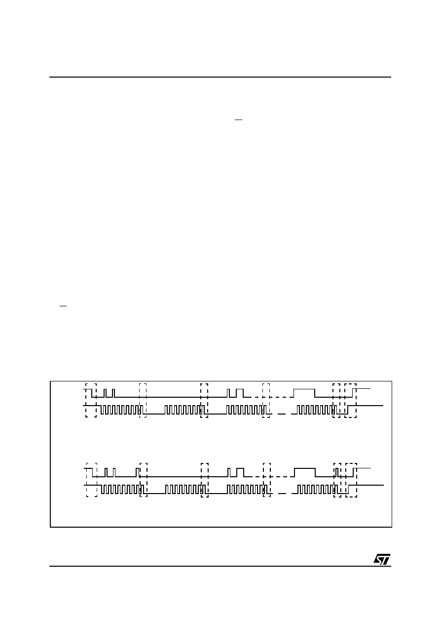
Figure 58. I2C Signal Diagram
SDA
SCL
Start
Ack
A0h
Device Slave Address
00h
Data Address
Ack
Data1(B0h)
DataN(F0h) Ack STOP
WRITE DATA TO I2C DEVICE (Slave Address A0h)
SDA
SCL
Start
Ack
A1h
Device Slave Address
Data1(00h) Ack
Ack
Data2(B0h)
DataN(F0h) Nack STOP
READ DATA FROM I2C DEVICE (Slave Address A1h)
相关PDF资料 |
PDF描述 |
|---|---|
| ST72E734J6D0 | 8-BIT, UVPROM, 8 MHz, MICROCONTROLLER, CDIP42 |
| ST72T774S9T1 | 8-BIT, OTPROM, 8 MHz, MICROCONTROLLER, PQFP44 |
| ST7294C6B6 | 8-BIT, MROM, 4 MHz, MICROCONTROLLER, PDIP28 |
| ST72T94C6M6 | 8-BIT, OTPROM, MICROCONTROLLER, PDSO28 |
| ST72C171K2B6 | 8-BIT, FLASH, 8 MHz, MICROCONTROLLER, PDIP32 |
相关代理商/技术参数 |
参数描述 |
|---|---|
| ST727X4-EMU2B | 制造商:STMicroelectronics 功能描述:REALTIME EMULATOR BOARD - Bulk |
| ST727X4-EPB/US | 制造商:STMicroelectronics 功能描述:PROGRAMMER - Bulk |
| ST-7-28 | 功能描述:XFRMR PWR 115V 14VAC 2.6A RoHS:是 类别:变压器 >> 功率 系列:ST 标准包装:1 系列:260 类型:标准 最大功率:65 VA 主线圈:双 副线圈:三路,中心抽头 在某电流时的串联输出电压:500 VAC @ 85mA,5 VAC @ 2A,6.3 VAC @ 2A 在某电流时的并联输出电压:- 安装类型:底座安装 尺寸/尺寸:102.36mm L x 67.31mm W 高度 - 座高(最大):66.80mm 端接类型:导线引线 |
| ST7-28 | 制造商:SUPERWORLD 制造商全称:Superworld Electronics 功能描述:POWER TRANSFORMER |
| ST7-28B56 | 功能描述:电源变压器 SPLIT BOBBIN HORZ MOUNT XFMR RoHS:否 制造商:Triad Magnetics 功率额定值:12 VA 初级电压额定值:115 V / 230 V 次级电压额定值:12 V / 24 V 安装风格:SMD/SMT 一次绕组:Dual Primary Winding 二次绕组:Dual Secondary Winding 长度:2.5 in 宽度:2 in 高度:1.062 in |
发布紧急采购,3分钟左右您将得到回复。