- 您现在的位置:买卖IC网 > PDF目录98145 > ST72774S9T1/XXX (STMICROELECTRONICS) 8-BIT, MROM, 8 MHz, MICROCONTROLLER, PQFP44 PDF资料下载
参数资料
| 型号: | ST72774S9T1/XXX |
| 厂商: | STMICROELECTRONICS |
| 元件分类: | 微控制器/微处理器 |
| 英文描述: | 8-BIT, MROM, 8 MHz, MICROCONTROLLER, PQFP44 |
| 封装: | TQFP-44 |
| 文件页数: | 3/144页 |
| 文件大小: | 1280K |
| 代理商: | ST72774S9T1/XXX |
第1页第2页当前第3页第4页第5页第6页第7页第8页第9页第10页第11页第12页第13页第14页第15页第16页第17页第18页第19页第20页第21页第22页第23页第24页第25页第26页第27页第28页第29页第30页第31页第32页第33页第34页第35页第36页第37页第38页第39页第40页第41页第42页第43页第44页第45页第46页第47页第48页第49页第50页第51页第52页第53页第54页第55页第56页第57页第58页第59页第60页第61页第62页第63页第64页第65页第66页第67页第68页第69页第70页第71页第72页第73页第74页第75页第76页第77页第78页第79页第80页第81页第82页第83页第84页第85页第86页第87页第88页第89页第90页第91页第92页第93页第94页第95页第96页第97页第98页第99页第100页第101页第102页第103页第104页第105页第106页第107页第108页第109页第110页第111页第112页第113页第114页第115页第116页第117页第118页第119页第120页第121页第122页第123页第124页第125页第126页第127页第128页第129页第130页第131页第132页第133页第134页第135页第136页第137页第138页第139页第140页第141页第142页第143页第144页
ST72774/ST727754/ST72734
100/144
DDC INTERFACE (Cont’d)
The Write and Read operations allow the EDID
data to be downloaded during factory alignment
(for example).
Writes to the memory by the DMA engine can be
inhibited by means of the WP bit in the DCR
register.
A write of the last data structure byte sets a flag
and may be programmed to generate an interrupt
request.
The Data address (sub-address) is either the
second byte of write transfers or is pointed to by
the
internal
address
counter
automatically
incremented after each byte transfer.
Physical address mapping of the data structure
within the memory space is performed with a
dedicated register accessible by software.
4.8.5.1.2 Mode description
DDC1 Mode: This mode is only enabled when the
DDC v2 or P&D-DDC v2 standards are validated. It
transmits only the EDID v1 data (128 bytes).
To switch the DDC1/2B Interface to DDC1 mode,
software must first clear the CF0 bit in the DCR
register while the HWPE bit=0 and then set the
HWPE bit to enable the DDC1/2B Interface.
A proper initialization sequence (see Figure 59)
must supply nine clock pulses on the VSYNCI pin
in order to internally synchronize the device.
During this initialization sequence, the SDA pin is
in high impedance. On the rising edge of the 10th
pulse applied on VSYNCI, the device outputs on
SDA the most significant (MSB) bit of the byte
located at data address 00h.
A byte is clocked out by means of 9 clock pulses
on Vsync, 8 clock pulses for the data byte itself and
an extra pulse for a Don’t Care bit.
As long as SCL is not held low, each byte of the
memory array is transmitted serially on SDA.
The internal address counter is incremented
automatically until the last byte is transmitted.
Then, it rolls over to relative location 00h.
The physical mapping of the data structure
depends on the configuration and on the content of
the AHR register which can be set by software
(see Figure 60).
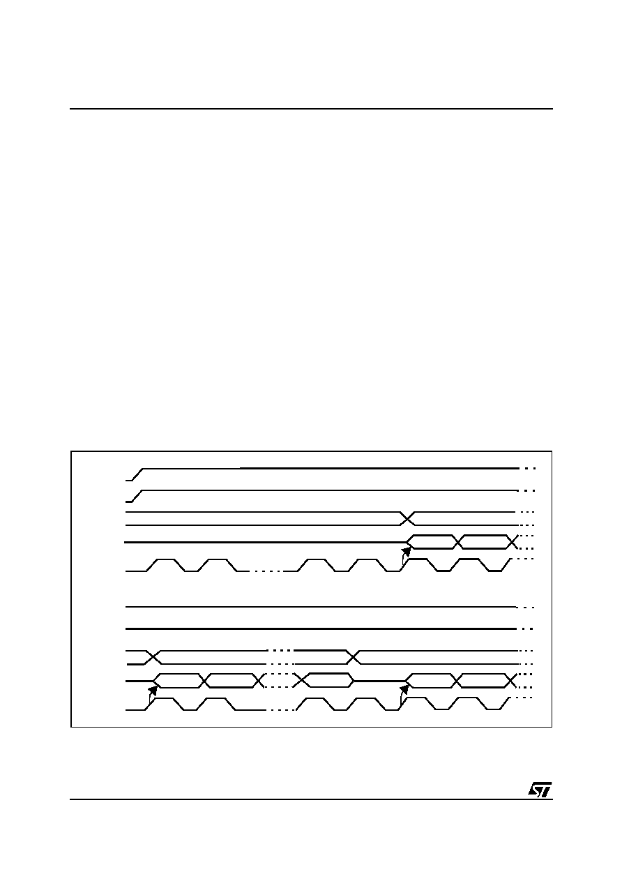
Figure 59. DDC1 Waveforms
Vsync
SDA
12
8
9
Bit 7
10
11
PE
SCL
Bit 6
ALR
00h
XX
Vsync
SDA
Bit 7
PE
SCL
Bit 6
ALR
00h
7Fh
Bit 7
Bit 6
Bit 0
相关PDF资料 |
PDF描述 |
|---|---|
| ST72E734J6D0 | 8-BIT, UVPROM, 8 MHz, MICROCONTROLLER, CDIP42 |
| ST72T774S9T1 | 8-BIT, OTPROM, 8 MHz, MICROCONTROLLER, PQFP44 |
| ST7294C6B6 | 8-BIT, MROM, 4 MHz, MICROCONTROLLER, PDIP28 |
| ST72T94C6M6 | 8-BIT, OTPROM, MICROCONTROLLER, PDSO28 |
| ST72C171K2B6 | 8-BIT, FLASH, 8 MHz, MICROCONTROLLER, PDIP32 |
相关代理商/技术参数 |
参数描述 |
|---|---|
| ST727X4-EMU2B | 制造商:STMicroelectronics 功能描述:REALTIME EMULATOR BOARD - Bulk |
| ST727X4-EPB/US | 制造商:STMicroelectronics 功能描述:PROGRAMMER - Bulk |
| ST-7-28 | 功能描述:XFRMR PWR 115V 14VAC 2.6A RoHS:是 类别:变压器 >> 功率 系列:ST 标准包装:1 系列:260 类型:标准 最大功率:65 VA 主线圈:双 副线圈:三路,中心抽头 在某电流时的串联输出电压:500 VAC @ 85mA,5 VAC @ 2A,6.3 VAC @ 2A 在某电流时的并联输出电压:- 安装类型:底座安装 尺寸/尺寸:102.36mm L x 67.31mm W 高度 - 座高(最大):66.80mm 端接类型:导线引线 |
| ST7-28 | 制造商:SUPERWORLD 制造商全称:Superworld Electronics 功能描述:POWER TRANSFORMER |
| ST7-28B56 | 功能描述:电源变压器 SPLIT BOBBIN HORZ MOUNT XFMR RoHS:否 制造商:Triad Magnetics 功率额定值:12 VA 初级电压额定值:115 V / 230 V 次级电压额定值:12 V / 24 V 安装风格:SMD/SMT 一次绕组:Dual Primary Winding 二次绕组:Dual Secondary Winding 长度:2.5 in 宽度:2 in 高度:1.062 in |
发布紧急采购,3分钟左右您将得到回复。