- 您现在的位置:买卖IC网 > PDF目录19517 > TMS320DM365ZCE30 (Texas Instruments)IC DIGITAL MEDIA SOC 338NFBGA PDF资料下载
参数资料
| 型号: | TMS320DM365ZCE30 |
| 厂商: | Texas Instruments |
| 文件页数: | 10/210页 |
| 文件大小: | 0K |
| 描述: | IC DIGITAL MEDIA SOC 338NFBGA |
| 标准包装: | 160 |
| 系列: | TMS320DM3x, DaVinci™ |
| 类型: | 数字媒体片内系统(DMSoC) |
| 接口: | EBI/EMI,以太网,I²C,McBSP,SPI,UART,USB |
| 时钟速率: | 300MHz |
| 非易失内存: | ROM(16 kB) |
| 芯片上RAM: | 56kB |
| 电压 - 输入/输出: | 1.8V,3.3V |
| 电压 - 核心: | 1.35V |
| 工作温度: | 0°C ~ 85°C |
| 安装类型: | 表面贴装 |
| 封装/外壳: | 338-LFBGA |
| 供应商设备封装: | 338-NFBGA(13x13) |
| 包装: | 托盘 |
| 其它名称: | 296-27979 TMS320DM365ZCE30-ND |
第1页第2页第3页第4页第5页第6页第7页第8页第9页当前第10页第11页第12页第13页第14页第15页第16页第17页第18页第19页第20页第21页第22页第23页第24页第25页第26页第27页第28页第29页第30页第31页第32页第33页第34页第35页第36页第37页第38页第39页第40页第41页第42页第43页第44页第45页第46页第47页第48页第49页第50页第51页第52页第53页第54页第55页第56页第57页第58页第59页第60页第61页第62页第63页第64页第65页第66页第67页第68页第69页第70页第71页第72页第73页第74页第75页第76页第77页第78页第79页第80页第81页第82页第83页第84页第85页第86页第87页第88页第89页第90页第91页第92页第93页第94页第95页第96页第97页第98页第99页第100页第101页第102页第103页第104页第105页第106页第107页第108页第109页第110页第111页第112页第113页第114页第115页第116页第117页第118页第119页第120页第121页第122页第123页第124页第125页第126页第127页第128页第129页第130页第131页第132页第133页第134页第135页第136页第137页第138页第139页第140页第141页第142页第143页第144页第145页第146页第147页第148页第149页第150页第151页第152页第153页第154页第155页第156页第157页第158页第159页第160页第161页第162页第163页第164页第165页第166页第167页第168页第169页第170页第171页第172页第173页第174页第175页第176页第177页第178页第179页第180页第181页第182页第183页第184页第185页第186页第187页第188页第189页第190页第191页第192页第193页第194页第195页第196页第197页第198页第199页第200页第201页第202页第203页第204页第205页第206页第207页第208页第209页第210页
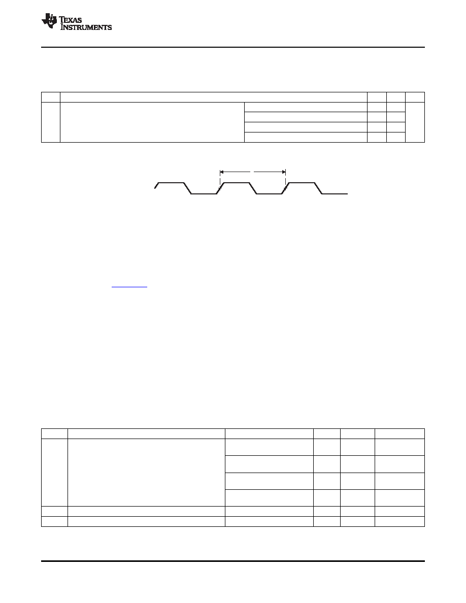
DDR_CLK
1
SPRS457E
– MARCH 2009 – REVISED JUNE 2011
6.10.3 DDR2 Memory Controller Electrical Data/Timing
Table 6-23. Switching Characteristics Over Recommended Operating Conditions for DDR2 Memory
Controller(1) (2)(see )
NO.
PARAMETER
MIN
MAX UNIT
1
tf(DDR_CLK)
Frequency, DDR_CLK
173-DDR2 (supported for 216-MHz device)
125
173
216-DDR2 (supported for 270-MHz device)
125
216
MHz
270-DDR2 (supported for 300-MHz device)
125
270
mDDR (supported for all devices)
90
168
(1)
DDR_CLK = PLLC1.SYSCLK7/2 or PLLC2.SYSCLK3/2.
(2)
The PLL2 Controller must be programmed such that the resulting DDR_CLK clock frequency is within the specified range.
Figure 6-18. DDR2 Memory Controller Clock Timing
6.10.3.1 DDR2/mDDR Interface
This section provides the timing specification for the DDR2/mDDR interface as a PCB design and
manufacturing specification. The design rules constrain PCB trace length, PCB trace skew, signal
integrity, cross-talk, and signal timing. These rules, when followed, result in a reliable DDR2/mDDR
memory system without the need for a complex timing closure process. For more information regarding
guidelines for using this DDR2 specification, Understanding TI's PCB Routing Rule-Based DDR2 Timing
Specification (SPRAAV0).
6.10.3.1.1 DDR2/mDDR Interface Schematic
Figure 6-19 shows the DDR2/mDDR interface schematic for a single-memory DDR2/mDDR system. The
dual-memory system shown in Figure 6-20. Pin numbers for the device can be obtained from the pin
description section.
6.10.3.1.2 Compatible JEDEC DDR2/mDDR Devices
Table 6-24 shows the parameters of the JEDEC DDR2/mDDR devices that are compatible with this
interface. Generally, the DDR2/mDDR interface is compatible with x16 DDR2/mDDR devices.
The device also supports JEDEC DDR2/mDDR x8 devices in the dual chip configuration. In this case, one
chip supplies the upper byte and the second chip supplies the lower byte. Addresses and most control
signals are shared just like regular dual chip memory configurations.
Table 6-24. Compatible JEDEC DDR2/mDDR Devices
No.
Parameter
Min
Max
Unit
Notes
1
JEDEC DDR2/mDDR Device Speed Grade
DDR2-400
See Notes (1),
(for 173MHz DDR2)
(2)
mDDR-400
See Notes (1),
(for 168MHz mDDR)
(3)
DDR2-533
See Notes (1),
(for 216MHz DDR2)
(2)
DDR2-667
See Notes (1),
(for 270MHz DDR2)
(2)
2
JEDEC DDR2/mDDR Device Bit Width
x8
x16
Bits
3
JEDEC DDR2/mDDR Device Count
1
2
Devices
See Note (4)
(1)
Higher DDR2/mDDR speed grades are supported due to inherent JEDEC DDR2/mDDR backwards compatibility.
(2)
Used for DDR2.
(3)
Used for mobile DDR.
(4)
Supported configurations are one 16-bit DDR2/mDDR memory or two 8-bit DDR2/mDDR memories.
Copyright
2009–2011, Texas Instruments Incorporated
Peripheral Information and Electrical Specifications
107
Product Folder Link(s): TMS320DM365
相关PDF资料 |
PDF描述 |
|---|---|
| EPM7256AETC144-5N | IC MAX 7000 CPLD 256 144-TQFP |
| VI-B0J-CY-F4 | CONVERTER MOD DC/DC 36V 50W |
| TPSR105M010R9000 | CAP TANT 1UF 10V 20% 0805 |
| EPM7256AETC144-7 | IC MAX 7000 CPLD 256 144-TQFP |
| ES3B-13-F | RECT SUPER FAST SMD 100V 3A SMC |
相关代理商/技术参数 |
参数描述 |
|---|---|
| TMS320DM365ZCED30 | 功能描述:处理器 - 专门应用 Digital Media SOC RoHS:否 制造商:Freescale Semiconductor 类型:Multimedia Applications 核心:ARM Cortex A9 处理器系列:i.MX6 数据总线宽度:32 bit 最大时钟频率:1 GHz 指令/数据缓存: 数据 RAM 大小:128 KB 数据 ROM 大小: 工作电源电压: 最大工作温度:+ 95 C 安装风格:SMD/SMT 封装 / 箱体:MAPBGA-432 |
| TMS320DM365ZCEF | 功能描述:处理器 - 专门应用 Dig Media System- on-Chip RoHS:否 制造商:Freescale Semiconductor 类型:Multimedia Applications 核心:ARM Cortex A9 处理器系列:i.MX6 数据总线宽度:32 bit 最大时钟频率:1 GHz 指令/数据缓存: 数据 RAM 大小:128 KB 数据 ROM 大小: 工作电源电压: 最大工作温度:+ 95 C 安装风格:SMD/SMT 封装 / 箱体:MAPBGA-432 |
| TMS320DM367ZCED | 制造商:Texas Instruments 功能描述:TMS320DM367ZCEF |
| TMS320DM367ZCED30 | 制造商:Texas Instruments 功能描述:TMS320DM367ZCEF |
| TMS320DM368ZCE | 功能描述:处理器 - 专门应用 Digital Media SOC RoHS:否 制造商:Freescale Semiconductor 类型:Multimedia Applications 核心:ARM Cortex A9 处理器系列:i.MX6 数据总线宽度:32 bit 最大时钟频率:1 GHz 指令/数据缓存: 数据 RAM 大小:128 KB 数据 ROM 大小: 工作电源电压: 最大工作温度:+ 95 C 安装风格:SMD/SMT 封装 / 箱体:MAPBGA-432 |
发布紧急采购,3分钟左右您将得到回复。