- 您现在的位置:买卖IC网 > PDF目录19517 > TMS320DM365ZCE30 (Texas Instruments)IC DIGITAL MEDIA SOC 338NFBGA PDF资料下载
参数资料
| 型号: | TMS320DM365ZCE30 |
| 厂商: | Texas Instruments |
| 文件页数: | 169/210页 |
| 文件大小: | 0K |
| 描述: | IC DIGITAL MEDIA SOC 338NFBGA |
| 标准包装: | 160 |
| 系列: | TMS320DM3x, DaVinci™ |
| 类型: | 数字媒体片内系统(DMSoC) |
| 接口: | EBI/EMI,以太网,I²C,McBSP,SPI,UART,USB |
| 时钟速率: | 300MHz |
| 非易失内存: | ROM(16 kB) |
| 芯片上RAM: | 56kB |
| 电压 - 输入/输出: | 1.8V,3.3V |
| 电压 - 核心: | 1.35V |
| 工作温度: | 0°C ~ 85°C |
| 安装类型: | 表面贴装 |
| 封装/外壳: | 338-LFBGA |
| 供应商设备封装: | 338-NFBGA(13x13) |
| 包装: | 托盘 |
| 其它名称: | 296-27979 TMS320DM365ZCE30-ND |
第1页第2页第3页第4页第5页第6页第7页第8页第9页第10页第11页第12页第13页第14页第15页第16页第17页第18页第19页第20页第21页第22页第23页第24页第25页第26页第27页第28页第29页第30页第31页第32页第33页第34页第35页第36页第37页第38页第39页第40页第41页第42页第43页第44页第45页第46页第47页第48页第49页第50页第51页第52页第53页第54页第55页第56页第57页第58页第59页第60页第61页第62页第63页第64页第65页第66页第67页第68页第69页第70页第71页第72页第73页第74页第75页第76页第77页第78页第79页第80页第81页第82页第83页第84页第85页第86页第87页第88页第89页第90页第91页第92页第93页第94页第95页第96页第97页第98页第99页第100页第101页第102页第103页第104页第105页第106页第107页第108页第109页第110页第111页第112页第113页第114页第115页第116页第117页第118页第119页第120页第121页第122页第123页第124页第125页第126页第127页第128页第129页第130页第131页第132页第133页第134页第135页第136页第137页第138页第139页第140页第141页第142页第143页第144页第145页第146页第147页第148页第149页第150页第151页第152页第153页第154页第155页第156页第157页第158页第159页第160页第161页第162页第163页第164页第165页第166页第167页第168页当前第169页第170页第171页第172页第173页第174页第175页第176页第177页第178页第179页第180页第181页第182页第183页第184页第185页第186页第187页第188页第189页第190页第191页第192页第193页第194页第195页第196页第197页第198页第199页第200页第201页第202页第203页第204页第205页第206页第207页第208页第209页第210页
SPRS457E
– MARCH 2009 – REVISED JUNE 2011
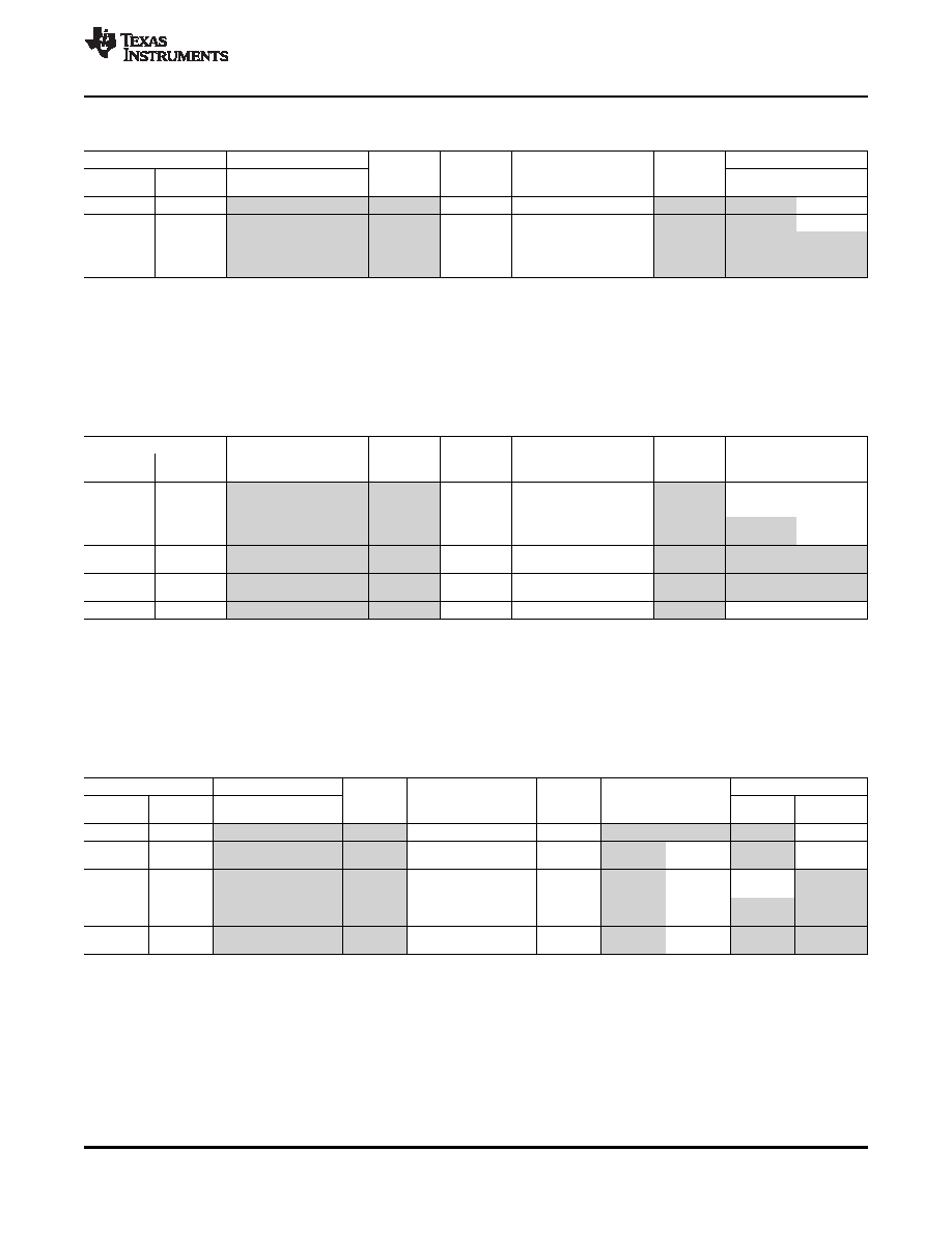
Table 3-7. 36-MHz Input Crystal Example(1)(2)(3)
PLL1
PLL2
ARM
DDR
MJCP
HDVICP
Voice Codec
(4)
Video Encoder
PLL Output
(2M/(N+1))
PLL Output
(2M/(N+1))
27MHz
74.25MHz
(5)(MHz)
(MHz)
345
230/24
432
12/1
216
172.5
-
1/16
-
432
12/1
270
30/4
270
216
1/66 (15.98kHz)
1/10
-
486
54/4
594
66/4
297
243
-
1/22
1/8
540
580/29
594
660/30
297
270
1/145 (16.002
1/22
1/8
kHz)
(1)
M = PLL controller multiplier. N = PLL controller divider.
(2)
All shaded frequencies derive from the PLL2 controller.
(3)
PLLC1SYSCLK4 (Configuration bus clock, peripheral system interfaces, EDMA) should be half of the PLLC1SYSCLK3 (MJCP and
HDVICP bus interface clock).
(4)
The Voice Codec divider value is the combination of the PLL controller 2 SYSCLK4 and Peripheral Clock Control Register PLLDIV2 bit
setting divider.
(5)
PLL Output is calculated by = Oscillator Input * (2M/(N+1)).
Table 3-8. 19.2-MHz Input Crystal Example(1)(2)(3)
PLL1
PLL2
ARM
DDR
MJCP
HDVICP
Voice Codec
(4)
Video Encoder
PLL Output
(5)
(2M/(N+1))
PLL Output
(2M/(N+1))
27MHz
74.25MHz
(MHz)
344.064
448/25
430.8
112/5
215.04
172.032
1/105
-
344.064
448/25
432
90/4
216
172.032
-
1/16
-
432
90/4
540
450/16
270
216
1/132 (15.98
1/20
-
KHz)
486
810/32
594
990/32
297
243
1/145
1/22
1/8
(16.002KHz)
540
450/16
594
990/32
297
270
1/145 (16.002
1/22
1/8
KHz)
540
450/16
593.92
464/15
296.96
270
1/145
1/20
-
(1)
M = PLL controller multiplier. N = PLL controller divider.
(2)
All shaded frequencies derive from the PLL2 controller.
(3)
PLLC1SYSCLK4 (Configuration bus clock, peripheral system interfaces, EDMA) should be half of the PLLC1SYSCLK3 (MJCP and
HDVICP bus interface clock).
(4)
The Voice Codec divider value is the combination of the PLL controller 2 SYSCLK4 and Peripheral Clock Control Register PLLDIV2 bit
setting divider.
(5)
PLL Output is calculated by = Oscillator Input * (2M/(N+1)).
Table 3-9. 27-MHz Input Crystal Example(1)(2)(3)
PLL1
PLL2
ARM
DDR
MJCP
HDVICP
Voice Codec
USB
Video Encoder
(4)
PLL Output
(5)
(2M/(N+1))
PLL Output
(2M/(N+1))
27 MHz
74.25 MHz
(MHz)
345.6
64/5
216
8/1
216
172.8
-
1/18 (24 MHz)
1/8
-
432
16/1
270
10/1
270
216
1/66 (15.98
1/18 (24MHz)
1/10
-
kHz)
432
16/1
519.75
154/8
259.875
216
1/127
1/18 (24MHz)
1/16
1/7
(15.98kHz)
492
164/9
594
22/1
297
246
1/145 (16.002 1/41 (12MHz)
1/22
1/8
kHz)
540
20/1
594
44/2
297
270
1/145 (16.002 1/45 (12MHz)
1/22
1/8
kHz)
(1)
M = PLL controller multiplier. N = PLL controller divider.
(2)
All shaded frequencies derive from the PLL2 controller.
(3)
PLLC1SYSCLK4 (Configuration bus clock, peripheral system interfaces, EDMA) should be half of the PLLC1SYSCLK3 (MJCP and
HDVICP bus interface clock).
(4)
The Voice Codec divider value is the combination of the PLL controller 2 SYSCLK4 and Peripheral Clock Control Register PLLDIV2 bit
setting divider.
(5)
PLL Output is calculated by = Oscillator Input * (2M/(N+1)).
Copyright
2009–2011, Texas Instruments Incorporated
Device Configurations
61
Product Folder Link(s): TMS320DM365
相关PDF资料 |
PDF描述 |
|---|---|
| EPM7256AETC144-5N | IC MAX 7000 CPLD 256 144-TQFP |
| VI-B0J-CY-F4 | CONVERTER MOD DC/DC 36V 50W |
| TPSR105M010R9000 | CAP TANT 1UF 10V 20% 0805 |
| EPM7256AETC144-7 | IC MAX 7000 CPLD 256 144-TQFP |
| ES3B-13-F | RECT SUPER FAST SMD 100V 3A SMC |
相关代理商/技术参数 |
参数描述 |
|---|---|
| TMS320DM365ZCED30 | 功能描述:处理器 - 专门应用 Digital Media SOC RoHS:否 制造商:Freescale Semiconductor 类型:Multimedia Applications 核心:ARM Cortex A9 处理器系列:i.MX6 数据总线宽度:32 bit 最大时钟频率:1 GHz 指令/数据缓存: 数据 RAM 大小:128 KB 数据 ROM 大小: 工作电源电压: 最大工作温度:+ 95 C 安装风格:SMD/SMT 封装 / 箱体:MAPBGA-432 |
| TMS320DM365ZCEF | 功能描述:处理器 - 专门应用 Dig Media System- on-Chip RoHS:否 制造商:Freescale Semiconductor 类型:Multimedia Applications 核心:ARM Cortex A9 处理器系列:i.MX6 数据总线宽度:32 bit 最大时钟频率:1 GHz 指令/数据缓存: 数据 RAM 大小:128 KB 数据 ROM 大小: 工作电源电压: 最大工作温度:+ 95 C 安装风格:SMD/SMT 封装 / 箱体:MAPBGA-432 |
| TMS320DM367ZCED | 制造商:Texas Instruments 功能描述:TMS320DM367ZCEF |
| TMS320DM367ZCED30 | 制造商:Texas Instruments 功能描述:TMS320DM367ZCEF |
| TMS320DM368ZCE | 功能描述:处理器 - 专门应用 Digital Media SOC RoHS:否 制造商:Freescale Semiconductor 类型:Multimedia Applications 核心:ARM Cortex A9 处理器系列:i.MX6 数据总线宽度:32 bit 最大时钟频率:1 GHz 指令/数据缓存: 数据 RAM 大小:128 KB 数据 ROM 大小: 工作电源电压: 最大工作温度:+ 95 C 安装风格:SMD/SMT 封装 / 箱体:MAPBGA-432 |
发布紧急采购,3分钟左右您将得到回复。