- 您现在的位置:买卖IC网 > PDF目录19517 > TMS320DM365ZCE30 (Texas Instruments)IC DIGITAL MEDIA SOC 338NFBGA PDF资料下载
参数资料
| 型号: | TMS320DM365ZCE30 |
| 厂商: | Texas Instruments |
| 文件页数: | 132/210页 |
| 文件大小: | 0K |
| 描述: | IC DIGITAL MEDIA SOC 338NFBGA |
| 标准包装: | 160 |
| 系列: | TMS320DM3x, DaVinci™ |
| 类型: | 数字媒体片内系统(DMSoC) |
| 接口: | EBI/EMI,以太网,I²C,McBSP,SPI,UART,USB |
| 时钟速率: | 300MHz |
| 非易失内存: | ROM(16 kB) |
| 芯片上RAM: | 56kB |
| 电压 - 输入/输出: | 1.8V,3.3V |
| 电压 - 核心: | 1.35V |
| 工作温度: | 0°C ~ 85°C |
| 安装类型: | 表面贴装 |
| 封装/外壳: | 338-LFBGA |
| 供应商设备封装: | 338-NFBGA(13x13) |
| 包装: | 托盘 |
| 其它名称: | 296-27979 TMS320DM365ZCE30-ND |
第1页第2页第3页第4页第5页第6页第7页第8页第9页第10页第11页第12页第13页第14页第15页第16页第17页第18页第19页第20页第21页第22页第23页第24页第25页第26页第27页第28页第29页第30页第31页第32页第33页第34页第35页第36页第37页第38页第39页第40页第41页第42页第43页第44页第45页第46页第47页第48页第49页第50页第51页第52页第53页第54页第55页第56页第57页第58页第59页第60页第61页第62页第63页第64页第65页第66页第67页第68页第69页第70页第71页第72页第73页第74页第75页第76页第77页第78页第79页第80页第81页第82页第83页第84页第85页第86页第87页第88页第89页第90页第91页第92页第93页第94页第95页第96页第97页第98页第99页第100页第101页第102页第103页第104页第105页第106页第107页第108页第109页第110页第111页第112页第113页第114页第115页第116页第117页第118页第119页第120页第121页第122页第123页第124页第125页第126页第127页第128页第129页第130页第131页当前第132页第133页第134页第135页第136页第137页第138页第139页第140页第141页第142页第143页第144页第145页第146页第147页第148页第149页第150页第151页第152页第153页第154页第155页第156页第157页第158页第159页第160页第161页第162页第163页第164页第165页第166页第167页第168页第169页第170页第171页第172页第173页第174页第175页第176页第177页第178页第179页第180页第181页第182页第183页第184页第185页第186页第187页第188页第189页第190页第191页第192页第193页第194页第195页第196页第197页第198页第199页第200页第201页第202页第203页第204页第205页第206页第207页第208页第209页第210页
SPRS457E
– MARCH 2009 – REVISED JUNE 2011
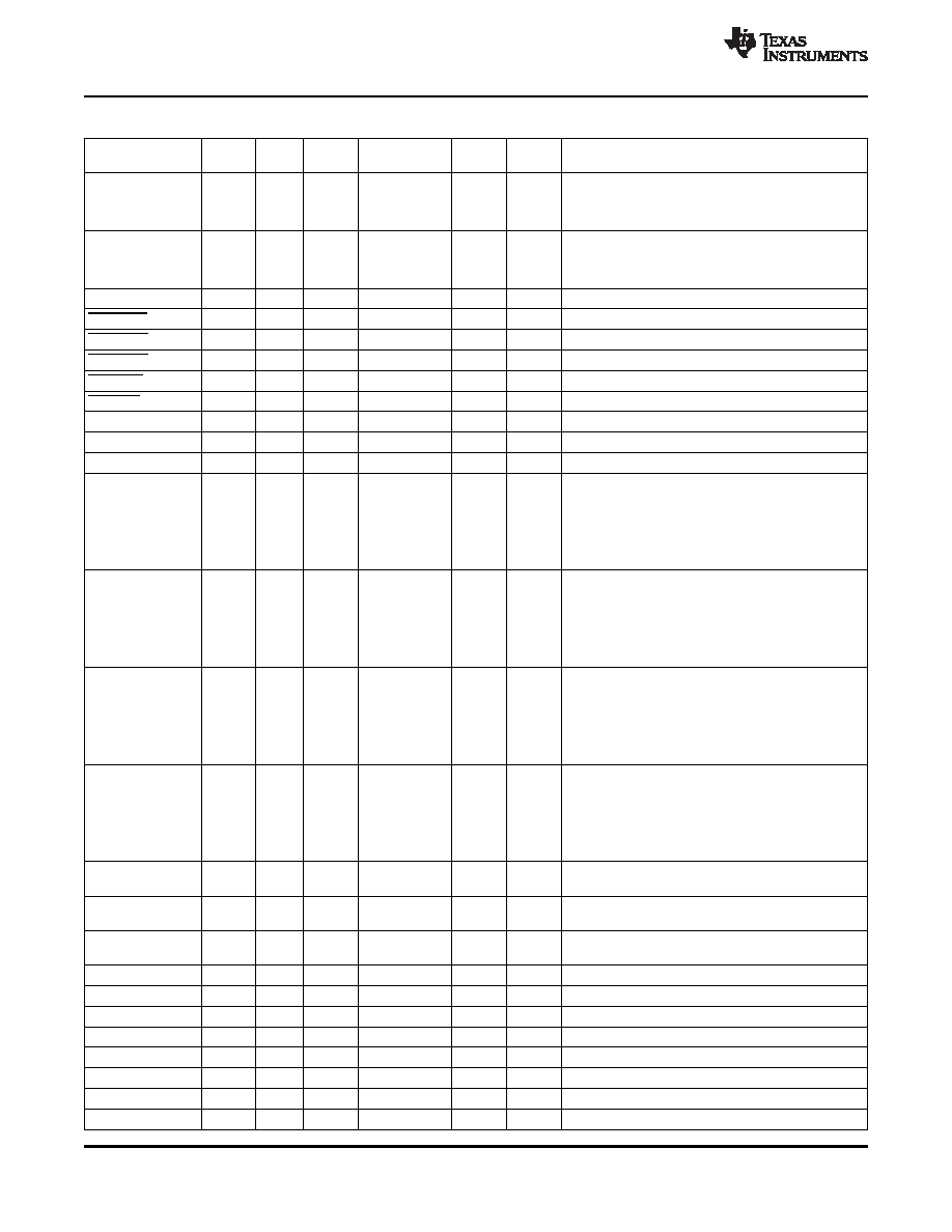
Table 2-5. Pin Descriptions (continued)
Name
BGA
Type
Group
Power
IPU
Reset
Description(4)
ID
(1)
Supply(2)
IPD(3)
State
VSSA18_DAC
E11
GND
Video
Video DAC: Analog 1.8-V ground
DAC
Note: If the DAC peripheral is not used, this pin must
be tied directly to VSS for proper device operation.
VSSA12_DAC
F11
GND
Video
Video DAC: Analog 1.2-V ground
DAC
Note: If the DAC peripheral is not used, this pin must
be tied directly to VSS for proper device operation.
DDR_CLK
W11
O
DDR
VDD18_DDR
DDR Data Clock
DDR_CLK
W12
O
DDR
VDD18_DDR
DDR Complementary Data Clock
DDR_RAS
U12
O
DDR
VDD18_DDR
DDR Row Address Strobe
DDR_CAS
V12
O
DDR
VDD18_DDR
DDR Column Address Strobe
DDR_WE
W13
O
DDR
VDD18_DDR
DDR Write Enable
DDR_CS
T12
O
DDR
VDD18_DDR
DDR Chip Select
DDR_CKE
R13
O
DDR
VDD18_DDR
DDR Clock Enable
DDR_DQM[1]
W6
O
DDR
VDD18_DDR
Data mask input for DDR_DQ[15:8]
DDR_DQM[0]
T11
O
DDR
VDD18_DDR
Data mask input for DDR_DQ[7:0]
DDR_DQS[1]
T7
I/O
DDR
VDD18_DDR
Data strobe input/outputs for each byte of the 16-bit
data bus used to synchronize the data transfers.
Output to DDR2 when writing and inputs when
reading. They are used to synchronize the data
transfers.
DDR_DQS1: For DDR_DQ[15:8]
DDR_DQS[0]
T10
I/O
DDR
VDD18_DDR
Data strobe input/outputs for each byte of the 16-bit
data bus used to synchronize the data transfers.
Output to DDR2 when writing and inputs when
reading. They are used to synchronize the data
transfers.
DDR_DQS0: For DDR_DQ[7:0]
DDR_DQSN[1]
U6
I/O
DDR
VDD18_DDR
DDR: Complimentary data strobe input/outputs for
each byte of the 16-bit data bus. They are outputs to
the DDR2 when writing and inputs when reading.
They are used to synchronize the data transfers.
Note: This signal is used in double ended differential
memory interfaces supported by the device.
DDR_DQSN[0]
U9
I/O
DDR
VDD18_DDR
DDR: Complimentary data strobe input/outputs for
each byte of the 16-bit data bus. They are outputs to
the DDR2 when writing and inputs when reading.
They are used to synchronize the data transfers.
Note: This signal is used in double ended differential
memory interfaces supported by the device.
DDR_BA[2]
V13
O
DDR
VDD18_DDR
Bank select outputs. Two are required for 1Gb DDR2
memories.
DDR_BA[1]
T13
O
DDR
VDD18_DDR
Bank select outputs. Two are required for 1Gb DDR2
memories.
DDR_BA[0]
W14
O
DDR
VDD18_DDR
Bank select outputs. Two are required for 1Gb DDR2
memories.
DDR_A13
T16
O
DDR
VDD18_DDR
DDR Address Bus bit 13
DDR_A12
V17
O
DDR
VDD18_DDR
DDR Address Bus bit 12
DDR_A11
W18
O
DDR
VDD18_DDR
DDR Address Bus bit 11
DDR_A10
V16
O
DDR
VDD18_DDR
DDR Address Bus bit 10
DDR_A9
U16
O
DDR
VDD18_DDR
DDR Address Bus bit 09
DDR_A8
W17
O
DDR
VDD18_DDR
DDR Address Bus bit 08
DDR_A7
T15
O
DDR
VDD18_DDR
DDR Address Bus bit 07
DDR_A6
W16
O
DDR
VDD18_DDR
DDR Address Bus bit 06
28
Device Overview
Copyright
2009–2011, Texas Instruments Incorporated
Product Folder Link(s): TMS320DM365
相关PDF资料 |
PDF描述 |
|---|---|
| EPM7256AETC144-5N | IC MAX 7000 CPLD 256 144-TQFP |
| VI-B0J-CY-F4 | CONVERTER MOD DC/DC 36V 50W |
| TPSR105M010R9000 | CAP TANT 1UF 10V 20% 0805 |
| EPM7256AETC144-7 | IC MAX 7000 CPLD 256 144-TQFP |
| ES3B-13-F | RECT SUPER FAST SMD 100V 3A SMC |
相关代理商/技术参数 |
参数描述 |
|---|---|
| TMS320DM365ZCED30 | 功能描述:处理器 - 专门应用 Digital Media SOC RoHS:否 制造商:Freescale Semiconductor 类型:Multimedia Applications 核心:ARM Cortex A9 处理器系列:i.MX6 数据总线宽度:32 bit 最大时钟频率:1 GHz 指令/数据缓存: 数据 RAM 大小:128 KB 数据 ROM 大小: 工作电源电压: 最大工作温度:+ 95 C 安装风格:SMD/SMT 封装 / 箱体:MAPBGA-432 |
| TMS320DM365ZCEF | 功能描述:处理器 - 专门应用 Dig Media System- on-Chip RoHS:否 制造商:Freescale Semiconductor 类型:Multimedia Applications 核心:ARM Cortex A9 处理器系列:i.MX6 数据总线宽度:32 bit 最大时钟频率:1 GHz 指令/数据缓存: 数据 RAM 大小:128 KB 数据 ROM 大小: 工作电源电压: 最大工作温度:+ 95 C 安装风格:SMD/SMT 封装 / 箱体:MAPBGA-432 |
| TMS320DM367ZCED | 制造商:Texas Instruments 功能描述:TMS320DM367ZCEF |
| TMS320DM367ZCED30 | 制造商:Texas Instruments 功能描述:TMS320DM367ZCEF |
| TMS320DM368ZCE | 功能描述:处理器 - 专门应用 Digital Media SOC RoHS:否 制造商:Freescale Semiconductor 类型:Multimedia Applications 核心:ARM Cortex A9 处理器系列:i.MX6 数据总线宽度:32 bit 最大时钟频率:1 GHz 指令/数据缓存: 数据 RAM 大小:128 KB 数据 ROM 大小: 工作电源电压: 最大工作温度:+ 95 C 安装风格:SMD/SMT 封装 / 箱体:MAPBGA-432 |
发布紧急采购,3分钟左右您将得到回复。