参数资料
| 型号: | TMS320DM647ZUT7 |
| 厂商: | Texas Instruments |
| 文件页数: | 108/190页 |
| 文件大小: | 0K |
| 描述: | IC DGTL MEDIA PROC 529-FCBGA |
| 标准包装: | 84 |
| 系列: | TMS320DM64x, DaVinci™ |
| 类型: | 定点 |
| 接口: | 主机接口,I²C,McASP,PCI,SPI,UART |
| 时钟速率: | 720MHz |
| 非易失内存: | ROM(64 kB) |
| 芯片上RAM: | 320kB |
| 电压 - 输入/输出: | 1.8V,3.3V |
| 电压 - 核心: | 1.20V |
| 工作温度: | 0°C ~ 85°C |
| 安装类型: | 表面贴装 |
| 封装/外壳: | 529-BFBGA,FCBGA |
| 供应商设备封装: | 529-FCBGA(19x19) |
| 包装: | 托盘 |
| 其它名称: | 296-34539-5 TMS320DM647ZUT7-ND |
第1页第2页第3页第4页第5页第6页第7页第8页第9页第10页第11页第12页第13页第14页第15页第16页第17页第18页第19页第20页第21页第22页第23页第24页第25页第26页第27页第28页第29页第30页第31页第32页第33页第34页第35页第36页第37页第38页第39页第40页第41页第42页第43页第44页第45页第46页第47页第48页第49页第50页第51页第52页第53页第54页第55页第56页第57页第58页第59页第60页第61页第62页第63页第64页第65页第66页第67页第68页第69页第70页第71页第72页第73页第74页第75页第76页第77页第78页第79页第80页第81页第82页第83页第84页第85页第86页第87页第88页第89页第90页第91页第92页第93页第94页第95页第96页第97页第98页第99页第100页第101页第102页第103页第104页第105页第106页第107页当前第108页第109页第110页第111页第112页第113页第114页第115页第116页第117页第118页第119页第120页第121页第122页第123页第124页第125页第126页第127页第128页第129页第130页第131页第132页第133页第134页第135页第136页第137页第138页第139页第140页第141页第142页第143页第144页第145页第146页第147页第148页第149页第150页第151页第152页第153页第154页第155页第156页第157页第158页第159页第160页第161页第162页第163页第164页第165页第166页第167页第168页第169页第170页第171页第172页第173页第174页第175页第176页第177页第178页第179页第180页第181页第182页第183页第184页第185页第186页第187页第188页第189页第190页
SPRS372H – MAY 2007 – REVISED APRIL 2012
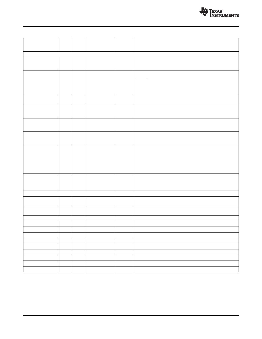
Table 2-4. Terminal Functions (continued)
TERMINAL NAME
NO
TYPE(
INTERNAL
OPER
DESCRIPTION
1)
PULLUP/
VOLT
PULLDOWN
CONFIGURATION AND EMIFA
DEVICEENABLE0/
F2
I/O/Z
IPD
3.3 V
EMIFA External Address 20 (word address). (O/Z) For proper
AEA20
device operation, this pin must be externally pulled up with a 1-k
resistor at device reset
EMIFAWIDTH/
G3
I/O/Z
IPD
3.3 V
EMIFA External Address 22 (word address). (O/Z) EMIFA data
AEA22
bus width selection pin state captured at the rising edge of
RESET.
0 - sets EMIFA CS2 to 8-bit data bus width
1 - sets EMIFA CS2 to 16 bit data bus width. For details, see
FASTBOOT/
G2
I/O/Z
IPD
3.3 V
EMIFA External Address 22 (word address). (O/Z) Enables FAST
AEA21
BOOT of the device. For details, see Section 3.
UHPIEN
H2
I
IPD
3.3 V
UHPI Enable Pin. This pin controls the selection (enable/disable)
of the HPI and GPIO[0:7] muxed with PCI. For details, see
HPIWIDTH/
H3
I/O/Z
IPD
3.3 V
EMIFA External Address 16 (word address) (O/Z) HPI peripheral
AEA16
bus width (HPI_WIDTH) select (Applies only when HPI is enabled;
UHPIEN pin = 1)
RSV_BOOT/
H6
I/O/Z
IPU
3.3 V
EMIFA External Address 15 (word address) (O/Z) For proper
AEA15
device operation, this pin must be externally pulled up with a 1-k
resistor at device reset.
PCI66/AEA18
G5
I/O/Z
IPD
3.3 V
PCI Frequency Selection (PCI66). The PCI peripheral must be
enabled (UHPIEN = 0) to use this function. PCI66_AEA18 selects
the PCI operating frequency of 66 MHz or 33 MHz. PCI operating
frequency is selected at reset via the pullup/pulldown resistor on
the PCI66 pin AEA18:
0 - PCI operates at 33 MHz (default)
1 - PCI operates at 66 MHz.
BOOTMODE0/AEA11
F3
I/O/Z
IPD
3.3 V
The BOOTMODE[3:0] defines what boot code is executed on
BOOTMODE1/AEA12
F4
device reset. See Section 3.2.1 for more details.
BOOTMODE2/AEA13
F5
BOOTMODE3/AEA14
G6
INTER-INTEGRATED CIRCUIT (I2C)
SCL
D22
I/O/Z
3.3 V
I2C clock. When the I2C module is used, use an external pullup
resistor.
SDA
C23
I/O/Z
3.3 V
I2C data. When I2C is used, make certain there is an external
pullup resistor.
SGMII0/1 and MDIO(1)(2)
SGMII0RXN
AA10
I
1.2 V
Differential SGMII Port 0 RX input (negative)
SGMII0RXP
AA9
I
1.2 V
Differential SGMII Port 0 RX input (positive)
SGMII0TXN
W11
O
1.2 V
Differential SGMII Port 0 TX output (negative)
SGMII0TXP
Y11
O
1.2 V
Differential SGMII Port 0 TX output (positive)
SGMII1RXN
AC9
I
1.2 V
Differential SGMII Port 1 RX input (negative)
SGMII1RXP
AB9
I
1.2 V
Differential SGMII Port 1 RX input (positive)
SGMII1TXN
W9
O
1.2 V
Differential SGMII Port 1 TX output (negative)
SGMII1TXP
W8
O
1.2 V
Differential SGMII Port 1 TX output (positive)
MDCLK
U9
OZ
IPD
3.3 V
MDIO Serial Clock (MDCLK)
(1)
For DM647: Leave the SGMII1RXP/N and SGMII1TXP/N pins disconnected. Disable ENTX/ENRX bits in CFGTX1/CFGRX1 for SGMII1
and still configure the CFGPLL because the SerDes TXBCLK0 is used as the internal VBUS clock. For DM648: if one of the SGMII pair
is not used, the same approach must be used.
(2)
If the Ethernet Subsystem is not used at all, these connections must be followed:
Disconnect AA10, AA9, W11,Y11, AC9, AB9, W9, W8, and U9
Connect AC11 to CVDD
Connect AB11 to VSS
Directly connect V11 (VDDA), W10 (VDDA), T10 (VDDD), U10 (VDDD) , AB8 (VDDT), U11 (VDDT), R9 (ESS core power), R11 (ESS core
power) to CVDD
Directly connect AB10, (VDDR) to DVDD18
24
Device Overview
Copyright 2007–2012, Texas Instruments Incorporated
Product Folder Link(s): TMS320DM647 TMS320DM648
相关PDF资料 |
PDF描述 |
|---|---|
| TMS320VC5409GGU100 | IC DIG SIG PROCESSOR 144-BGA |
| TMS470R1A384PZQ | IC RISC MCU 384K FLASH 100-LQFP |
| TMX320DM365BZCE | IC DIGITAL MEDIA SOC 338NFBGA |
| TMX320F28069UPFPA | IC MCU 32BIT 128KB FLASH 80HTQFP |
| TPS2371PWRG4 | IC PWR INTRFCE SW FOR POE 8TSSOP |
相关代理商/技术参数 |
参数描述 |
|---|---|
| TMS320DM647ZUT9 | 功能描述:数字信号处理器和控制器 - DSP, DSC Dig Media Proc RoHS:否 制造商:Microchip Technology 核心:dsPIC 数据总线宽度:16 bit 程序存储器大小:16 KB 数据 RAM 大小:2 KB 最大时钟频率:40 MHz 可编程输入/输出端数量:35 定时器数量:3 设备每秒兆指令数:50 MIPs 工作电源电压:3.3 V 最大工作温度:+ 85 C 封装 / 箱体:TQFP-44 安装风格:SMD/SMT |
| TMS320DM647ZUTA8 | 功能描述:数字信号处理器和控制器 - DSP, DSC Digital Media Proc RoHS:否 制造商:Microchip Technology 核心:dsPIC 数据总线宽度:16 bit 程序存储器大小:16 KB 数据 RAM 大小:2 KB 最大时钟频率:40 MHz 可编程输入/输出端数量:35 定时器数量:3 设备每秒兆指令数:50 MIPs 工作电源电压:3.3 V 最大工作温度:+ 85 C 封装 / 箱体:TQFP-44 安装风格:SMD/SMT |
| TMS320DM647ZUTD1 | 制造商:Texas Instruments 功能描述:- Trays |
| TMS320DM647ZUTD7 | 功能描述:数字信号处理器和控制器 - DSP, DSC Digital Media Proc RoHS:否 制造商:Microchip Technology 核心:dsPIC 数据总线宽度:16 bit 程序存储器大小:16 KB 数据 RAM 大小:2 KB 最大时钟频率:40 MHz 可编程输入/输出端数量:35 定时器数量:3 设备每秒兆指令数:50 MIPs 工作电源电压:3.3 V 最大工作温度:+ 85 C 封装 / 箱体:TQFP-44 安装风格:SMD/SMT |
| TMS320DM647ZUTD9 | 功能描述:数字信号处理器和控制器 - DSP, DSC Digital Media Proc RoHS:否 制造商:Microchip Technology 核心:dsPIC 数据总线宽度:16 bit 程序存储器大小:16 KB 数据 RAM 大小:2 KB 最大时钟频率:40 MHz 可编程输入/输出端数量:35 定时器数量:3 设备每秒兆指令数:50 MIPs 工作电源电压:3.3 V 最大工作温度:+ 85 C 封装 / 箱体:TQFP-44 安装风格:SMD/SMT |
发布紧急采购,3分钟左右您将得到回复。