参数资料
| 型号: | TMS320DM647ZUT7 |
| 厂商: | Texas Instruments |
| 文件页数: | 4/190页 |
| 文件大小: | 0K |
| 描述: | IC DGTL MEDIA PROC 529-FCBGA |
| 标准包装: | 84 |
| 系列: | TMS320DM64x, DaVinci™ |
| 类型: | 定点 |
| 接口: | 主机接口,I²C,McASP,PCI,SPI,UART |
| 时钟速率: | 720MHz |
| 非易失内存: | ROM(64 kB) |
| 芯片上RAM: | 320kB |
| 电压 - 输入/输出: | 1.8V,3.3V |
| 电压 - 核心: | 1.20V |
| 工作温度: | 0°C ~ 85°C |
| 安装类型: | 表面贴装 |
| 封装/外壳: | 529-BFBGA,FCBGA |
| 供应商设备封装: | 529-FCBGA(19x19) |
| 包装: | 托盘 |
| 其它名称: | 296-34539-5 TMS320DM647ZUT7-ND |
第1页第2页第3页当前第4页第5页第6页第7页第8页第9页第10页第11页第12页第13页第14页第15页第16页第17页第18页第19页第20页第21页第22页第23页第24页第25页第26页第27页第28页第29页第30页第31页第32页第33页第34页第35页第36页第37页第38页第39页第40页第41页第42页第43页第44页第45页第46页第47页第48页第49页第50页第51页第52页第53页第54页第55页第56页第57页第58页第59页第60页第61页第62页第63页第64页第65页第66页第67页第68页第69页第70页第71页第72页第73页第74页第75页第76页第77页第78页第79页第80页第81页第82页第83页第84页第85页第86页第87页第88页第89页第90页第91页第92页第93页第94页第95页第96页第97页第98页第99页第100页第101页第102页第103页第104页第105页第106页第107页第108页第109页第110页第111页第112页第113页第114页第115页第116页第117页第118页第119页第120页第121页第122页第123页第124页第125页第126页第127页第128页第129页第130页第131页第132页第133页第134页第135页第136页第137页第138页第139页第140页第141页第142页第143页第144页第145页第146页第147页第148页第149页第150页第151页第152页第153页第154页第155页第156页第157页第158页第159页第160页第161页第162页第163页第164页第165页第166页第167页第168页第169页第170页第171页第172页第173页第174页第175页第176页第177页第178页第179页第180页第181页第182页第183页第184页第185页第186页第187页第188页第189页第190页
SPRS372H – MAY 2007 – REVISED APRIL 2012
6.9.2
DDR2 Memory Controller Peripheral Registers
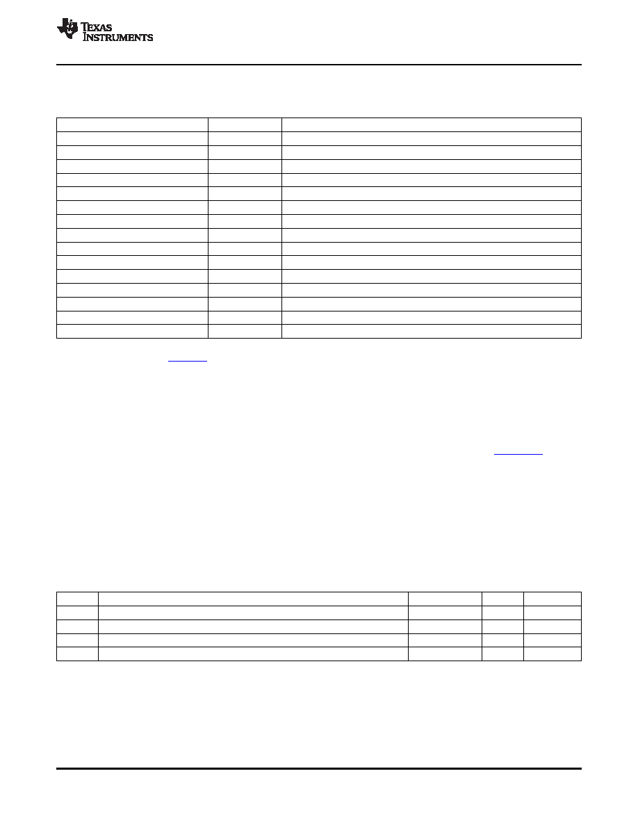
Table 6-28. DDR2 Memory Controller Registers(1)
HEX ADDRESS RANGE
ACRONYM
REGISTER NAME
0x7800 0000
MIDR
DDR2 Memory Controller Module and Revision Register
0x7800 0004
DMCSTAT
DDR2 Memory Controller Status Register
0x7800 0008
SDCFG
DDR2 Memory Controller SDRAM Configuration Register
0x7800 000C
SDRFC
DDR2 Memory Controller SDRAM Refresh Control Register
0x7800 0010
SDTIM1
DDR2 Memory Controller SDRAM Timing 1 Register
0x7800 0014
SDTIM2
DDR2 Memory Controller SDRAM Timing 2 Register
0x7800 0018
-
Reserved
0x7800 0020
BPRIO
DDR2 Memory Controller Burst Priority Register
0x7800 0024 - 0x7800 004C
-
Reserved
0x7800 0050 - 0x7800 0078
-
Reserved
0x7800 007C - 0x7800 00BC
-
Reserved
0x7800 00C0 - 0x7800 00E0
-
Reserved
0x7800 00E4
DMCCTL
DDR2 Memory Controller Control Register
0x7800 00E8 - 0x7800 00FC
-
Reserved
0x7800 0100 - 0x7FFF FFFF
-
Reserved
(1)
For details about the DDR2 registers and their modes, see the TMS320DM647/DM648 DSP DDR2 Memory Controller (DDR2) User's
Guide (literature number SPRUEK5).
6.9.3
DDR2 Interface
This section provides the timing information for the DDR2 interface as a PCB design and manufacturing
specification. The design rules constrain PCB trace length, PCB trace skew, signal integrity, cross-talk,
and signal timing. These rules, when followed, result in a reliable DDR2 memory system without the need
for a complex timing closure process. For more information regarding guidelines for using this DDR2
specification, Understanding TI's PCB Routing Rule-Based DDR2 Timing Specification (SPRAAV0).
6.9.3.1
DDR2 Interface Schematic
Figure 6-11 shows the DDR2 interface schematic for a x32 DDR2 memory system. The x16 DDR2 system
schematic shown in Figure 6-12 is identical except that the high word DDR2 device is deleted.
6.9.3.2
Compatible JEDEC DDR2 Devices
Table 6-29 shows the parameters of the JEDEC DDR2 devices that are compatible with this interface.
Generally, the DDR2 interface is compatible with x16 DDR2-533 speed grade DDR2 devices.
Table 6-29. Compatible JEDEC DDR2 Devices
NO.
PARAMETER
MIN
MAX
UNIT
1
JEDEC DDR2 Device Speed Grade(1)
DDR2-533
2
JEDEC DDR2 Device Bit Width
x16
Bits
3
JEDEC DDR2 Device Count(2)
1
2
Devices
4
JEDEC DDR2 Device Ball Count(3)
84
92
Balls
(1)
Higher DDR2 speed grades are supported due to inherent JEDEC DDR2 backwards compatibility.
(2)
One DDR2 device is used for 16-bit DDR2 memory system. Two DDR2 devices are used for 32-bit DDR2 memory system.
(3)
92 ball devices retained for legacy support. New designs will migrate to 84 ball DDR2 devices. Electrically, the 92 and 84 ball DDR2
devices are the same.
Copyright 2007–2012, Texas Instruments Incorporated
Peripheral Information and Electrical Specifications
101
Product Folder Link(s): TMS320DM647 TMS320DM648
相关PDF资料 |
PDF描述 |
|---|---|
| TMS320VC5409GGU100 | IC DIG SIG PROCESSOR 144-BGA |
| TMS470R1A384PZQ | IC RISC MCU 384K FLASH 100-LQFP |
| TMX320DM365BZCE | IC DIGITAL MEDIA SOC 338NFBGA |
| TMX320F28069UPFPA | IC MCU 32BIT 128KB FLASH 80HTQFP |
| TPS2371PWRG4 | IC PWR INTRFCE SW FOR POE 8TSSOP |
相关代理商/技术参数 |
参数描述 |
|---|---|
| TMS320DM647ZUT9 | 功能描述:数字信号处理器和控制器 - DSP, DSC Dig Media Proc RoHS:否 制造商:Microchip Technology 核心:dsPIC 数据总线宽度:16 bit 程序存储器大小:16 KB 数据 RAM 大小:2 KB 最大时钟频率:40 MHz 可编程输入/输出端数量:35 定时器数量:3 设备每秒兆指令数:50 MIPs 工作电源电压:3.3 V 最大工作温度:+ 85 C 封装 / 箱体:TQFP-44 安装风格:SMD/SMT |
| TMS320DM647ZUTA8 | 功能描述:数字信号处理器和控制器 - DSP, DSC Digital Media Proc RoHS:否 制造商:Microchip Technology 核心:dsPIC 数据总线宽度:16 bit 程序存储器大小:16 KB 数据 RAM 大小:2 KB 最大时钟频率:40 MHz 可编程输入/输出端数量:35 定时器数量:3 设备每秒兆指令数:50 MIPs 工作电源电压:3.3 V 最大工作温度:+ 85 C 封装 / 箱体:TQFP-44 安装风格:SMD/SMT |
| TMS320DM647ZUTD1 | 制造商:Texas Instruments 功能描述:- Trays |
| TMS320DM647ZUTD7 | 功能描述:数字信号处理器和控制器 - DSP, DSC Digital Media Proc RoHS:否 制造商:Microchip Technology 核心:dsPIC 数据总线宽度:16 bit 程序存储器大小:16 KB 数据 RAM 大小:2 KB 最大时钟频率:40 MHz 可编程输入/输出端数量:35 定时器数量:3 设备每秒兆指令数:50 MIPs 工作电源电压:3.3 V 最大工作温度:+ 85 C 封装 / 箱体:TQFP-44 安装风格:SMD/SMT |
| TMS320DM647ZUTD9 | 功能描述:数字信号处理器和控制器 - DSP, DSC Digital Media Proc RoHS:否 制造商:Microchip Technology 核心:dsPIC 数据总线宽度:16 bit 程序存储器大小:16 KB 数据 RAM 大小:2 KB 最大时钟频率:40 MHz 可编程输入/输出端数量:35 定时器数量:3 设备每秒兆指令数:50 MIPs 工作电源电压:3.3 V 最大工作温度:+ 85 C 封装 / 箱体:TQFP-44 安装风格:SMD/SMT |
发布紧急采购,3分钟左右您将得到回复。