- 您现在的位置:买卖IC网 > PDF目录297644 > UPSD3253B-40T6 (STMICROELECTRONICS) 8-BIT, FLASH, 40 MHz, MICROCONTROLLER, PQFP52 PDF资料下载
参数资料
| 型号: | UPSD3253B-40T6 |
| 厂商: | STMICROELECTRONICS |
| 元件分类: | 微控制器/微处理器 |
| 英文描述: | 8-BIT, FLASH, 40 MHz, MICROCONTROLLER, PQFP52 |
| 封装: | PLASTIC, TQFP-52 |
| 文件页数: | 23/189页 |
| 文件大小: | 1638K |
| 代理商: | UPSD3253B-40T6 |
第1页第2页第3页第4页第5页第6页第7页第8页第9页第10页第11页第12页第13页第14页第15页第16页第17页第18页第19页第20页第21页第22页当前第23页第24页第25页第26页第27页第28页第29页第30页第31页第32页第33页第34页第35页第36页第37页第38页第39页第40页第41页第42页第43页第44页第45页第46页第47页第48页第49页第50页第51页第52页第53页第54页第55页第56页第57页第58页第59页第60页第61页第62页第63页第64页第65页第66页第67页第68页第69页第70页第71页第72页第73页第74页第75页第76页第77页第78页第79页第80页第81页第82页第83页第84页第85页第86页第87页第88页第89页第90页第91页第92页第93页第94页第95页第96页第97页第98页第99页第100页第101页第102页第103页第104页第105页第106页第107页第108页第109页第110页第111页第112页第113页第114页第115页第116页第117页第118页第119页第120页第121页第122页第123页第124页第125页第126页第127页第128页第129页第130页第131页第132页第133页第134页第135页第136页第137页第138页第139页第140页第141页第142页第143页第144页第145页第146页第147页第148页第149页第150页第151页第152页第153页第154页第155页第156页第157页第158页第159页第160页第161页第162页第163页第164页第165页第166页第167页第168页第169页第170页第171页第172页第173页第174页第175页第176页第177页第178页第179页第180页第181页第182页第183页第184页第185页第186页第187页第188页第189页
Obsolete
Product(s)
- Obsolete
Product(s)
UPSD3254A, UPSD3254BV, UPSD3253B, UPSD3253BV
Memory blocks
119/189
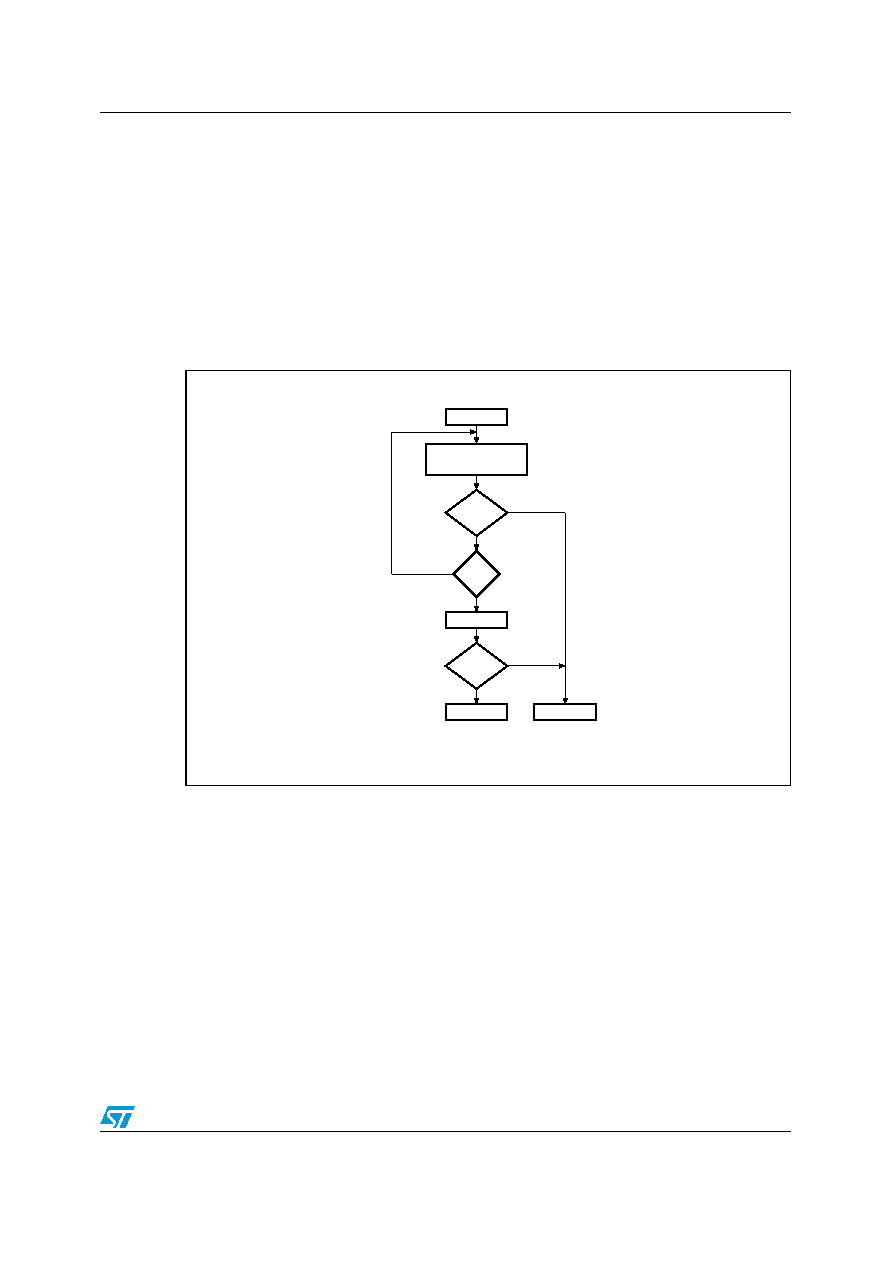
It is suggested (as with all Flash memories) to read the location again after the embedded
programming algorithm has completed, to compare the byte that was written to Flash
memory with the byte that was intended to be written.
When using the Data Toggle method after an Erase cycle, Figure 52 still applies. the Toggle
Flag bit (DQ6) toggles until the Erase cycle is complete. A 1 on the Error Flag bit (DQ5)
indicates a time-out condition on the Erase cycle; a '0' indicates no error. The MCU can read
any location within the sector being erased to get the Toggle Flag bit (DQ6) and the Error
Flag bit (DQ5).
PSDsoft Express generates ANSI C code functions which implement these Data Toggling
algorithms.
Figure 52.
Data toggle flowchart
22.6.3
Unlock Bypass
The Unlock Bypass instructions allow the system to program bytes to the Flash memories
faster than using the standard Program instruction. The Unlock Bypass mode is entered by
first initiating two Unlock cycles. This is followed by a third WRITE cycle containing the
Unlock Bypass code, 20h (as shown in Table 85).
The Flash memory then enters the Unlock Bypass mode. A two-cycle Unlock Bypass
Program instruction is all that is required to program in this mode. The first cycle in this
instruction contains the Unlock Bypass Program code, A0h. The second cycle contains the
program address and data. Additional data is programmed in the same manner. These
instructions dispense with the initial two Unlock cycles required in the standard Program
instruction, resulting in faster total Flash memory programming.
During the Unlock Bypass mode, only the Unlock Bypass Program and Unlock Bypass
Reset Flash instructions are valid.
READ
DQ5 & DQ6
START
READ DQ6
FAIL
PASS
AI01370B
DQ6
=
TOGGLE
NO
YES
DQ5
= 1
NO
YES
DQ6
=
TOGGLE
相关PDF资料 |
PDF描述 |
|---|---|
| UPSD3334D-40U6 | 8-BIT, FLASH, 40 MHz, MICROCONTROLLER, PQFP80 |
| US1001FL | 0.5 A, 100 V, SILICON, SIGNAL DIODE |
| US1A-HE3 | 1 A, 50 V, SILICON, SIGNAL DIODE, DO-214AC |
| US1B-HE3 | 1 A, 100 V, SILICON, SIGNAL DIODE, DO-214AC |
| US1G-HE3 | 1 A, 400 V, SILICON, SIGNAL DIODE, DO-214AC |
相关代理商/技术参数 |
参数描述 |
|---|---|
| UPSD3253B-40T6T | 制造商:STMICROELECTRONICS 制造商全称:STMicroelectronics 功能描述:Flash Programmable System Device with 8032 Microcontroller Core |
| UPSD3253B-40U1 | 制造商:STMICROELECTRONICS 制造商全称:STMicroelectronics 功能描述:Flash Programmable System Device with 8032 Microcontroller Core |
| UPSD3253B-40U1T | 制造商:STMICROELECTRONICS 制造商全称:STMicroelectronics 功能描述:Flash Programmable System Device with 8032 Microcontroller Core |
| UPSD3253B-40U6 | 制造商:STMICROELECTRONICS 制造商全称:STMicroelectronics 功能描述:Flash Programmable System Device with 8032 Microcontroller Core |
| UPSD3253B-40U6T | 制造商:STMICROELECTRONICS 制造商全称:STMicroelectronics 功能描述:Flash Programmable System Device with 8032 Microcontroller Core |
发布紧急采购,3分钟左右您将得到回复。