- 您现在的位置:买卖IC网 > PDF目录68583 > WJLXT971ALE.A4SE000 (CORTINA SYSTEMS INC) DATACOM, ETHERNET TRANSCEIVER, PQFP64 PDF资料下载
参数资料
| 型号: | WJLXT971ALE.A4SE000 |
| 厂商: | CORTINA SYSTEMS INC |
| 元件分类: | 网络接口 |
| 英文描述: | DATACOM, ETHERNET TRANSCEIVER, PQFP64 |
| 封装: | LEAD FREE, LQFP-64 |
| 文件页数: | 26/116页 |
| 文件大小: | 1172K |
| 代理商: | WJLXT971ALE.A4SE000 |
第1页第2页第3页第4页第5页第6页第7页第8页第9页第10页第11页第12页第13页第14页第15页第16页第17页第18页第19页第20页第21页第22页第23页第24页第25页当前第26页第27页第28页第29页第30页第31页第32页第33页第34页第35页第36页第37页第38页第39页第40页第41页第42页第43页第44页第45页第46页第47页第48页第49页第50页第51页第52页第53页第54页第55页第56页第57页第58页第59页第60页第61页第62页第63页第64页第65页第66页第67页第68页第69页第70页第71页第72页第73页第74页第75页第76页第77页第78页第79页第80页第81页第82页第83页第84页第85页第86页第87页第88页第89页第90页第91页第92页第93页第94页第95页第96页第97页第98页第99页第100页第101页第102页第103页第104页第105页第106页第107页第108页第109页第110页第111页第112页第113页第114页第115页第116页
LXT971A 3.3V Dual-Speed Fast Ethernet Transceiver
Datasheet
17
Document #: 249414
Revision #: 002
Rev. Date: August 7, 2002
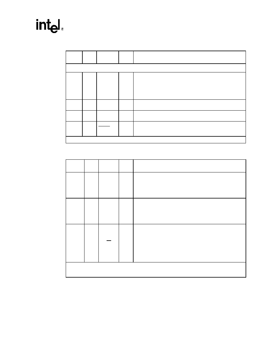
MII Control Interface Pins
D3
3
MDDIS
I
Management Disable. When MDDIS is High, the MDIO is disabled
from read and write operations.
When MDDIS is Low at power-up or reset, the Hardware Control
Interface pins control only the initial or “default” values of their
respective register bits. After the power-up/reset cycle is complete,
bit control reverts to the MDIO serial channel.
E7
43
MDC
I
Management Data Clock. Clock for the MDIO serial data channel.
Maximum frequency is 8 MHz.
D8
42
MDIO
I/O
Management Data Input/Output. Bidirectional serial data channel
for PHY/STA communication.
A1
64
MDINT
OD
Management Data Interrupt. When Register bit 18.1 = 1, an active
Low output on this pin indicates status change. Interrupt is cleared
by reading Register 19.
Table 3. LXT971A Network Interface Signal Descriptions
PBGA
Pin#
LQFP
Pin#
Symbol
Type1
Signal Description
H2
H3
19
20
TPFOP
TPFON
O
Twisted-Pair/Fiber Outputs, Positive & Negative.
During 100BASE-TX or 10BASE-T operation, TPFOP/N pins drive
802.3 compliant pulses onto the line.
During 100BASE-FX operation, TPFOP/N pins produce differential
LVPECL outputs for fiber transceivers.
H4
H5
23
24
TPFIP
TPFIN
I
Twisted-Pair/Fiber Inputs, Positive & Negative.
During 100BASE-TX or 10BASE-T operation, TPFIP/N pins receive
differential 100BASE-TX or 10BASE-T signals from the line.
During 100BASE-FX operation, TPFIP/N pins receive differential
LVPECL inputs from fiber transceivers.
G2
26
SD/TP
I
Signal Detect2: Dual function input depending on the state of the
device.
Reset and Power-Up. Media mode selection:
Tie High for FX mode (Register bit 16.0 = 1)
Tie Low for TP mode (Register bit 16.0 = 0)
Normal Operation (FX Mode): SD input from the fiber transceiver.
Normal Operation (TP Mode): Tie to GND (uses an internal pull-
down).
1. Type Column Coding: I = Input, O = Output, A = Analog, OD = Open Drain
2. For standard digital loopback testing (Register bit 0.14) in FX mode, the SD pin should be tied to an
LVPECL logic High (2.4 V).
Table 2. LXT971A MII Signal Descriptions (Continued)
PBGA
Pin#
LQFP
Pin#
Symbol
Type1
Signal Description
1. Type Column Coding: I = Input, O = Output, A = Analog, OD = Open Drain
相关PDF资料 |
PDF描述 |
|---|---|
| WJLXT971ALE.A4SE001 | DATACOM, ETHERNET TRANSCEIVER, PQFP64 |
| WJLXT971ALC.A4 | DATACOM, ETHERNET TRANSCEIVER, PQFP64 |
| WJLXT971ALE.A4 | DATACOM, ETHERNET TRANSCEIVER, PQFP64 |
| WJLXT971ALC.A4 | DATACOM, ETHERNET TRANSCEIVER, PQFP64 |
| WJLXT971ALE.A4 | DATACOM, ETHERNET TRANSCEIVER, PQFP64 |
相关代理商/技术参数 |
参数描述 |
|---|---|
| WJLXT971CA4 | 制造商:Intel 功能描述: |
| WJLXT972ALC.A4 | 功能描述:IC TRANS 3.3V ETHERNET 64-LQFP RoHS:是 类别:集成电路 (IC) >> 接口 - 驱动器,接收器,收发器 系列:- 产品培训模块:Lead (SnPb) Finish for COTS Obsolescence Mitigation Program 标准包装:25 系列:- 类型:收发器 驱动器/接收器数:2/2 规程:RS232 电源电压:4.5 V ~ 5.5 V 安装类型:通孔 封装/外壳:16-DIP(0.300",7.62mm) 供应商设备封装:16-PDIP 包装:管件 |
| WJLXT972ALC.A4 S E001 | 制造商:Intel 功能描述:PHY 1-CH 10Mbps/100Mbps 64-Pin LQFP T/R |
| WJLXT972ALC.A4-857341 | 功能描述:TXRX ETH 10/100 SGL PORT 64-LQFP RoHS:是 类别:集成电路 (IC) >> 接口 - 驱动器,接收器,收发器 系列:- 产品培训模块:Lead (SnPb) Finish for COTS Obsolescence Mitigation Program 标准包装:50 系列:- 类型:收发器 驱动器/接收器数:1/1 规程:RS422,RS485 电源电压:4.75 V ~ 5.25 V 安装类型:通孔 封装/外壳:8-DIP(0.300",7.62mm) 供应商设备封装:8-PDIP 包装:管件 产品目录页面:1402 (CN2011-ZH PDF) |
| WJLXT972ALC.A4-857345 | 功能描述:TXRX ETH 10/100 SGL PORT 64-LQFP RoHS:是 类别:集成电路 (IC) >> 接口 - 驱动器,接收器,收发器 系列:- 标准包装:1 系列:- 类型:线路收发器 驱动器/接收器数:5/3 规程:RS232 电源电压:3 V ~ 5.5 V 安装类型:表面贴装 封装/外壳:28-SOIC(0.295",7.50mm 宽) 供应商设备封装:28-SOIC 包装:Digi-Reel® 产品目录页面:918 (CN2011-ZH PDF) 其它名称:296-25096-6 |
发布紧急采购,3分钟左右您将得到回复。