参数资料
| 型号: | XA3S400A-4FGG400Q |
| 厂商: | Xilinx Inc |
| 文件页数: | 47/57页 |
| 文件大小: | 0K |
| 描述: | IC FPGA SPARTAN-3A 400K 400-FBGA |
| 产品培训模块: | Extended Spartan 3A FPGA Family |
| 标准包装: | 1 |
| 系列: | Spartan®-3A XA |
| LAB/CLB数: | 896 |
| 逻辑元件/单元数: | 8064 |
| RAM 位总计: | 368640 |
| 输入/输出数: | 311 |
| 门数: | 400000 |
| 电源电压: | 1.14 V ~ 1.26 V |
| 安装类型: | 表面贴装 |
| 工作温度: | -40°C ~ 125°C |
| 封装/外壳: | 400-BGA |
| 供应商设备封装: | 400-FBGA(21x21) |
第1页第2页第3页第4页第5页第6页第7页第8页第9页第10页第11页第12页第13页第14页第15页第16页第17页第18页第19页第20页第21页第22页第23页第24页第25页第26页第27页第28页第29页第30页第31页第32页第33页第34页第35页第36页第37页第38页第39页第40页第41页第42页第43页第44页第45页第46页当前第47页第48页第49页第50页第51页第52页第53页第54页第55页第56页第57页
XA Spartan-3A Automotive FPGA Family Data Sheet
DS681 (v2.0) April 22, 2011
Product Specification
51
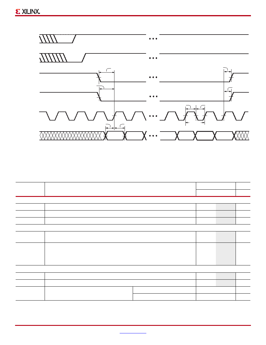
Slave Parallel Mode Timing
X-Ref Target - Figure 13
Figure 13: Waveforms for Slave Parallel Configuration
Table 50: Timing for the Slave Parallel Configuration Mode
Symbol
Description
Speed Grade: -4
Units
Min
Max
Setup Times
TSMDCC(2)
The time from the setup of data at the D0-D7 pins to the rising transition at the CCLK pin
7
–ns
TSMCSCC
Setup time on the CSI_B pin before the rising transition at the CCLK pin
7
–ns
TSMCCW
Setup time on the RDWR_B pin before the rising transition at the CCLK pin
15
–ns
Hold Times
TSMCCD
The time from the rising transition at the CCLK pin to the point when data is last held at
the D0-D7 pins
1.0
–ns
TSMCCCS
The time from the rising transition at the CCLK pin to the point when a logic level is last
held at the CSO_B pin
0
–ns
TSMWCC
The time from the rising transition at the CCLK pin to the point when a logic level is last
held at the RDWR_B pin
0
–ns
Clock Timing
TCCH
The High pulse width at the CCLK input pin
5
–ns
TCCL
The Low pulse width at the CCLK input pin
5
–ns
FCCPAR
Frequency of the clock signal at the CCLK input
pin
No bitstream compression
0
80
MHz
With bitstream compression
0
80
MHz
Notes:
1.
The numbers in this table are based on the operating conditions set forth in Table 8.
2.
Some Xilinx documents refer to Parallel modes as “SelectMAP” modes.
DS681_11_041111
Byte 0
Byte 1
Byte n
Byte n+1
T
SMWCC
1/F
CCPAR
T
SMCCCS
T
SCCH
T
SMCCW
T
SMCCD
T
SMCSCC
T
SMDCC
PROG_B
(Input)
(Open-Drain)
INIT_B
(Input)
CSI_B
RDWR_B
(Input)
CCLK
(Inputs)
D0 - D7
T
MCCH
T
SCCL
T
MCCL
Notes:
1.
It is possible to abort configuration by pulling CSI_B Low in a given CCLK cycle, then switching RDWR_B Low or High in any subsequent
cycle for which CSI_B remains Low. The RDWR_B pin asynchronously controls the driver impedance of the D0–D7 bus. When RDWR_B
switches High, be careful to avoid contention on the D0–D7 bus.
相关PDF资料 |
PDF描述 |
|---|---|
| XC2V80-4FG256I | IC FPGA VIRTEX-II 256FGBGA |
| RMM43DTAH | CONN EDGECARD 86POS R/A .156 SLD |
| 25AA080AT-I/MS | IC EEPROM 8KBIT 10MHZ 8MSOP |
| XC3SD1800A-4FGG676I | SPARTAN-3ADSP FPGA 1800K 676FBGA |
| 25LC080A-I/MS | IC EEPROM 8KBIT 10MHZ 8MSOP |
相关代理商/技术参数 |
参数描述 |
|---|---|
| XA3S400A-4FTG256I | 功能描述:IC FPGA SPARTAN-3A 400K 256FTBGA RoHS:是 类别:集成电路 (IC) >> 嵌入式 - FPGA(现场可编程门阵列) 系列:Spartan®-3A XA 标准包装:40 系列:Spartan® 6 LX LAB/CLB数:3411 逻辑元件/单元数:43661 RAM 位总计:2138112 输入/输出数:358 门数:- 电源电压:1.14 V ~ 1.26 V 安装类型:表面贴装 工作温度:-40°C ~ 100°C 封装/外壳:676-BGA 供应商设备封装:676-FBGA(27x27) |
| XA3S400A-4FTG256Q | 功能描述:IC FPGA SPARTAN-3A 400K 256FTBGA RoHS:是 类别:集成电路 (IC) >> 嵌入式 - FPGA(现场可编程门阵列) 系列:Spartan®-3A XA 标准包装:40 系列:Spartan® 6 LX LAB/CLB数:3411 逻辑元件/单元数:43661 RAM 位总计:2138112 输入/输出数:358 门数:- 电源电压:1.14 V ~ 1.26 V 安装类型:表面贴装 工作温度:-40°C ~ 100°C 封装/外壳:676-BGA 供应商设备封装:676-FBGA(27x27) |
| XA3S500E | 制造商:XILINX 制造商全称:XILINX 功能描述:XA Spartan-3E Automotive FPGA Family Data Sheet |
| XA3S500E-4CPG132I | 功能描述:IC FPGA SPARTAN-3E 500K 132CSBGA RoHS:是 类别:集成电路 (IC) >> 嵌入式 - FPGA(现场可编程门阵列) 系列:Spartan®-3E XA 标准包装:40 系列:Spartan® 6 LX LAB/CLB数:3411 逻辑元件/单元数:43661 RAM 位总计:2138112 输入/输出数:358 门数:- 电源电压:1.14 V ~ 1.26 V 安装类型:表面贴装 工作温度:-40°C ~ 100°C 封装/外壳:676-BGA 供应商设备封装:676-FBGA(27x27) |
| XA3S500E-4CPG132Q | 功能描述:IC FPGA SPARTAN-3E 500K 132CSBGA RoHS:是 类别:集成电路 (IC) >> 嵌入式 - FPGA(现场可编程门阵列) 系列:Spartan®-3E XA 标准包装:40 系列:Spartan® 6 LX LAB/CLB数:3411 逻辑元件/单元数:43661 RAM 位总计:2138112 输入/输出数:358 门数:- 电源电压:1.14 V ~ 1.26 V 安装类型:表面贴装 工作温度:-40°C ~ 100°C 封装/外壳:676-BGA 供应商设备封装:676-FBGA(27x27) |
发布紧急采购,3分钟左右您将得到回复。