参数资料
| 型号: | XC3S700AN-4FG484I |
| 厂商: | Xilinx Inc |
| 文件页数: | 43/123页 |
| 文件大小: | 0K |
| 描述: | IC FPGA SPARTAN 3AN 484FBGA |
| 标准包装: | 60 |
| 系列: | Spartan®-3AN |
| LAB/CLB数: | 1472 |
| 逻辑元件/单元数: | 13248 |
| RAM 位总计: | 368640 |
| 输入/输出数: | 372 |
| 门数: | 700000 |
| 电源电压: | 1.14 V ~ 1.26 V |
| 安装类型: | 表面贴装 |
| 工作温度: | -40°C ~ 100°C |
| 封装/外壳: | 484-BBGA |
| 供应商设备封装: | 484-FBGA |
第1页第2页第3页第4页第5页第6页第7页第8页第9页第10页第11页第12页第13页第14页第15页第16页第17页第18页第19页第20页第21页第22页第23页第24页第25页第26页第27页第28页第29页第30页第31页第32页第33页第34页第35页第36页第37页第38页第39页第40页第41页第42页当前第43页第44页第45页第46页第47页第48页第49页第50页第51页第52页第53页第54页第55页第56页第57页第58页第59页第60页第61页第62页第63页第64页第65页第66页第67页第68页第69页第70页第71页第72页第73页第74页第75页第76页第77页第78页第79页第80页第81页第82页第83页第84页第85页第86页第87页第88页第89页第90页第91页第92页第93页第94页第95页第96页第97页第98页第99页第100页第101页第102页第103页第104页第105页第106页第107页第108页第109页第110页第111页第112页第113页第114页第115页第116页第117页第118页第119页第120页第121页第122页第123页
Spartan-3AN FPGA Family: DC and Switching Characteristics
DS557 (v4.1) April 1, 2011
Product Specification
26
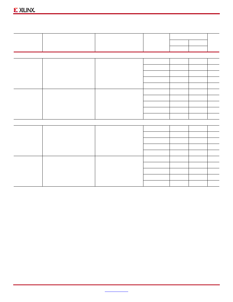
Pin-to-Pin Setup and Hold Times
Table 22: Pin-to-Pin Setup and Hold Times for the IOB Input Path (System Synchronous)
Symbol
Description
Conditions
Device
Speed Grade
Units
-5
-4
Min
Setup Times
TPSDCM
When writing to the Input
Flip-Flop (IFF), the time from the
setup of data at the Input pin to
the active transition at a Global
Clock pin. The DCM is in use. No
Input Delay is programmed.
LVCMOS25(2),
IFD_DELAY_VALUE = 0,
with DCM(4)
XC3S50AN
2.45
2.68
ns
XC3S200AN
2.59
2.84
ns
XC3S400AN
2.38
2.68
ns
XC3S700AN
2.38
2.57
ns
XC3S1400AN
1.91
2.17
ns
TPSFD
When writing to IFF, the time from
the setup of data at the Input pin
to an active transition at the
Global Clock pin. The DCM is not
in use. The Input Delay is
programmed.
LVCMOS25(2),
IFD_DELAY_VALUE = 5,
without DCM
XC3S50AN
2.55
2.76
ns
XC3S200AN
2.32
2.76
ns
XC3S400AN
2.21
2.60
ns
XC3S700AN
2.28
2.63
ns
XC3S1400AN
2.33
2.41
ns
Hold Times
TPHDCM
When writing to IFF, the time from
the active transition at the Global
Clock pin to the point when data
must be held at the Input pin. The
DCM is in use. No Input Delay is
programmed.
LVCMOS25(3),
IFD_DELAY_VALUE = 0,
with DCM(4)
XC3S50AN
–0.36
ns
XC3S200AN
–0.52
ns
XC3S400AN
–0.33
–0.29
ns
XC3S700AN
–0.17
–0.12
ns
XC3S1400AN
–0.07
0.00
ns
TPHFD
When writing to IFF, the time from
the active transition at the Global
Clock pin to the point when data
must be held at the Input pin. The
DCM is not in use. The Input
Delay is programmed.
LVCMOS25(3),
IFD_DELAY_VALUE = 5,
without DCM
XC3S50AN
–0.63
–0.58
ns
XC3S200AN
–0.56
ns
XC3S400AN
–0.42
ns
XC3S700AN
–0.80
–0.75
ns
XC3S1400AN
–0.69
ns
Notes:
1.
The numbers in this table are tested using the methodology presented in Table 30 and are based on the operating conditions set forth in
2.
This setup time requires adjustment whenever a signal standard other than LVCMOS25 is assigned to the Global Clock Input or the data
Input. If this is true of the Global Clock Input, subtract the appropriate adjustment from Table 26. If this is true of the data Input, add the
appropriate Input adjustment from the same table.
3.
This hold time requires adjustment whenever a signal standard other than LVCMOS25 is assigned to the Global Clock Input or the data
Input. If this is true of the Global Clock Input, add the appropriate Input adjustment from Table 26. If this is true of the data Input, subtract the
appropriate Input adjustment from the same table. When the hold time is negative, it is possible to change the data before the clock’s active
edge.
4.
DCM output jitter is included in all measurements.
相关PDF资料 |
PDF描述 |
|---|---|
| 84981-4 | CONN FFC 4POS 1MM RT ANG SMD |
| XC5VTX240T-2FFG1759CES | IC FPGA VIRTEX5TX 240K 1759FBGA |
| ABB70DHBN | CONN EDGECARD 140PS R/A .050 SLD |
| XC5VTX240T-2FF1759CES | IC FPGA VIRTEX5TX 240K 1759FBGA |
| ABB70DHBD | CONN EDGECARD 140PS R/A .050 SLD |
相关代理商/技术参数 |
参数描述 |
|---|---|
| XC3S700AN-4FGG484C | 功能描述:IC SPARTAN-3AN FPGA 700K 484FBGA RoHS:是 类别:集成电路 (IC) >> 嵌入式 - FPGA(现场可编程门阵列) 系列:Spartan®-3AN 标准包装:60 系列:XP LAB/CLB数:- 逻辑元件/单元数:10000 RAM 位总计:221184 输入/输出数:244 门数:- 电源电压:1.71 V ~ 3.465 V 安装类型:表面贴装 工作温度:0°C ~ 85°C 封装/外壳:388-BBGA 供应商设备封装:388-FPBGA(23x23) 其它名称:220-1241 |
| XC3S700AN-4FGG484CES | 制造商:Xilinx 功能描述: |
| XC3S700AN-4FGG484I | 功能描述:IC FPGA SPARTAN -3AN700K 484FBGA RoHS:是 类别:集成电路 (IC) >> 嵌入式 - FPGA(现场可编程门阵列) 系列:Spartan®-3AN 标准包装:24 系列:ECP2 LAB/CLB数:1500 逻辑元件/单元数:12000 RAM 位总计:226304 输入/输出数:131 门数:- 电源电压:1.14 V ~ 1.26 V 安装类型:表面贴装 工作温度:0°C ~ 85°C 封装/外壳:208-BFQFP 供应商设备封装:208-PQFP(28x28) |
| XC3S700AN-5FG484C | 制造商:Xilinx 功能描述:FPGA SPARTAN-3AN FAMILY 700K GATES 13248 CELLS 770MHZ 90NM T - Trays 制造商:Xilinx 功能描述:IC FPGA 372 I/O 484FBGA |
| XC3S700AN-5FGG484C | 功能描述:IC FPGA SPARTAN-3A 700K 484-FBGA RoHS:是 类别:集成电路 (IC) >> 嵌入式 - FPGA(现场可编程门阵列) 系列:Spartan®-3AN 标准包装:40 系列:Spartan® 6 LX LAB/CLB数:3411 逻辑元件/单元数:43661 RAM 位总计:2138112 输入/输出数:358 门数:- 电源电压:1.14 V ~ 1.26 V 安装类型:表面贴装 工作温度:-40°C ~ 100°C 封装/外壳:676-BGA 供应商设备封装:676-FBGA(27x27) |
发布紧急采购,3分钟左右您将得到回复。