- 您现在的位置:买卖IC网 > PDF目录300163 > ZL30108LDG1 (XILINX INC) ATM/SONET/SDH SUPPORT CIRCUIT, QCC32 PDF资料下载
参数资料
| 型号: | ZL30108LDG1 |
| 厂商: | XILINX INC |
| 元件分类: | 数字传输电路 |
| 英文描述: | ATM/SONET/SDH SUPPORT CIRCUIT, QCC32 |
| 封装: | 5 X 5 MM, 0.90 MM HEIGHT, 0.50 MM PITCH, LEAD FREE, MO-220, QFN-32 |
| 文件页数: | 27/57页 |
| 文件大小: | 691K |
| 代理商: | ZL30108LDG1 |
第1页第2页第3页第4页第5页第6页第7页第8页第9页第10页第11页第12页第13页第14页第15页第16页第17页第18页第19页第20页第21页第22页第23页第24页第25页第26页当前第27页第28页第29页第30页第31页第32页第33页第34页第35页第36页第37页第38页第39页第40页第41页第42页第43页第44页第45页第46页第47页第48页第49页第50页第51页第52页第53页第54页第55页第56页第57页
ZL30108
Data Sheet
6
Zarlink Semiconductor Inc.
3.0
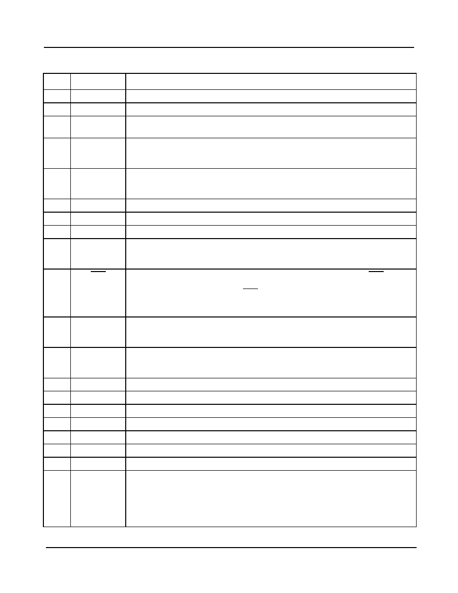
Pin Description
Pin #
Name
Description
1GND
Ground. 0V
2VCORE
Positive Supply Voltage. +1.8 VDC nominal
3LOCK
Lock Indicator (Output). This output goes to a logic high when the PLL is frequency
locked to the selected input reference.
4
REF_FAIL0
Reference 0 Failure Indicator (Output). A logic high at this pin indicates that the REF0
reference frequency has exceeded the out-of-range limit set by the OOR_SEL pin or that
it is exhibiting abrupt phase or frequency changes.
5
REF_FAIL1
Reference 1 Failure Indicator (Output). A logic high at this pin indicates that the REF1
reference frequency has exceeded the out-of-range limit set by the OOR_SEL pin or that
it is exhibiting abrupt phase or frequency changes.
6VCORE
Positive Supply Voltage. +1.8 VDC nominal.
7AVCORE
Positive Analog Supply Voltage. +1.8 VDC nominal.
8GND
Ground. 0V
9
MODE_SEL
Mode Select (Input). This input determines the mode of operation: See Table 3.
0: Normal mode (device locked to input reference)
1: Freerun mode
10
RST
Reset (Input). A logic low at this input resets the device. On power up, the RST pin must
be held low for a minimum of 300 ns after the power supply pins have reached the
minimum supply voltage. When the RST pin goes high, the device will transition into a
Reset state for 3 ms. In the Reset state all clock and frame pulse outputs will be forced
into high impedance.
11
OSCo
Oscillator Master Clock (Output). For crystal operation, a 20 MHz crystal is connected
from this pin to OSCi. This output is not suitable for driving other devices. For clock
oscillator operation, this pin must be left unconnected.
12
OSCi
Oscillator Master Clock (Input). For crystal operation, a 20 MHz crystal is connected
from this pin to OSCo. For clock oscillator operation, this pin must be connected to a
clock source.
13
IC
Internal Connection. Connect this pin to VDD.
14
VDD
Positive Supply Voltage. +3.3 VDC nominal
15
AVDD
Positive Analog Supply Voltage. +3.3 VDC nominal
16
GND
Ground. 0V
17
AGND
Analog Ground. 0V
18
AVCORE
Positive Analog Supply Voltage. +1.8 VDC nominal
19
AVDD
Positive Analog Supply Voltage. +3.3 VDC nominal
20
F2ko
Multi Frame Pulse (Output). This is a CMOS 2 kHz active high 51 ns framing pulse,
which marks the beginning of a multi frame.
This clock output pad includes a Schmitt triggered input which serves as a PLL feedback
path; proper transmission-line termination should be applied to maintain reflections below
Schmitt trigger levels.
相关PDF资料 |
PDF描述 |
|---|---|
| ZL30316GKG2 | SPECIALTY TELECOM CIRCUIT, PBGA256 |
| ZL30316GKG | SPECIALTY TELECOM CIRCUIT, PBGA256 |
| ZL30402/QCC1 | ATM/SONET/SDH SUPPORT CIRCUIT, PQFP80 |
| ZL30402/QCG1 | ATM/SONET/SDH SUPPORT CIRCUIT, PQFP80 |
| ZL50112GAG2 | SPECIALTY TELECOM CIRCUIT, PBGA552 |
相关代理商/技术参数 |
参数描述 |
|---|---|
| ZL30109 | 制造商:ZARLINK 制造商全称:Zarlink Semiconductor Inc 功能描述:DS1/E1 System Synchronizer with 19.44 MHz Output |
| ZL30109_05 | 制造商:ZARLINK 制造商全称:Zarlink Semiconductor Inc 功能描述:DS1/E1 System Synchronizer with |
| ZL30109QDG | 制造商:Microsemi Corporation 功能描述: |
| ZL30109QDG1 | 制造商:Microsemi Corporation 功能描述:DS1/E1 System Synchronizer 64-Pin TQFP 制造商:Microsemi Corporation 功能描述:DS1/E1 SYS. SYNCH WITH 19.44MHZ 制造商:Microsemi Corporation 功能描述:DS1/E1 SYS SYNCHRONIZER 64TQFP - Trays 制造商:MICROSEMI CONSUMER MEDICAL PRODUCT GROUP 功能描述:IC SYNCHRONIZER DPLL 64TQFP 制造商:Microsemi Corporation 功能描述:IC SYNCHRONIZER DPLL 64TQFP |
| ZL30110 | 制造商:ZARLINK 制造商全称:Zarlink Semiconductor Inc 功能描述:Telecom Rate Conversion DPLL |
发布紧急采购,3分钟左右您将得到回复。