- 您现在的位置:买卖IC网 > PDF目录278507 > ZPSD813F3V-20J 1M X 1 FLASH, 27 I/O, PIA-GENERAL PURPOSE, PQCC52 PDF资料下载
参数资料
| 型号: | ZPSD813F3V-20J |
| 元件分类: | 微控制器/微处理器 |
| 英文描述: | 1M X 1 FLASH, 27 I/O, PIA-GENERAL PURPOSE, PQCC52 |
| 封装: | PLASTIC, LDCC-52 |
| 文件页数: | 7/132页 |
| 文件大小: | 513K |
| 代理商: | ZPSD813F3V-20J |
第1页第2页第3页第4页第5页第6页当前第7页第8页第9页第10页第11页第12页第13页第14页第15页第16页第17页第18页第19页第20页第21页第22页第23页第24页第25页第26页第27页第28页第29页第30页第31页第32页第33页第34页第35页第36页第37页第38页第39页第40页第41页第42页第43页第44页第45页第46页第47页第48页第49页第50页第51页第52页第53页第54页第55页第56页第57页第58页第59页第60页第61页第62页第63页第64页第65页第66页第67页第68页第69页第70页第71页第72页第73页第74页第75页第76页第77页第78页第79页第80页第81页第82页第83页第84页第85页第86页第87页第88页第89页第90页第91页第92页第93页第94页第95页第96页第97页第98页第99页第100页第101页第102页第103页第104页第105页第106页第107页第108页第109页第110页第111页第112页第113页第114页第115页第116页第117页第118页第119页第120页第121页第122页第123页第124页第125页第126页第127页第128页第129页第130页第131页第132页
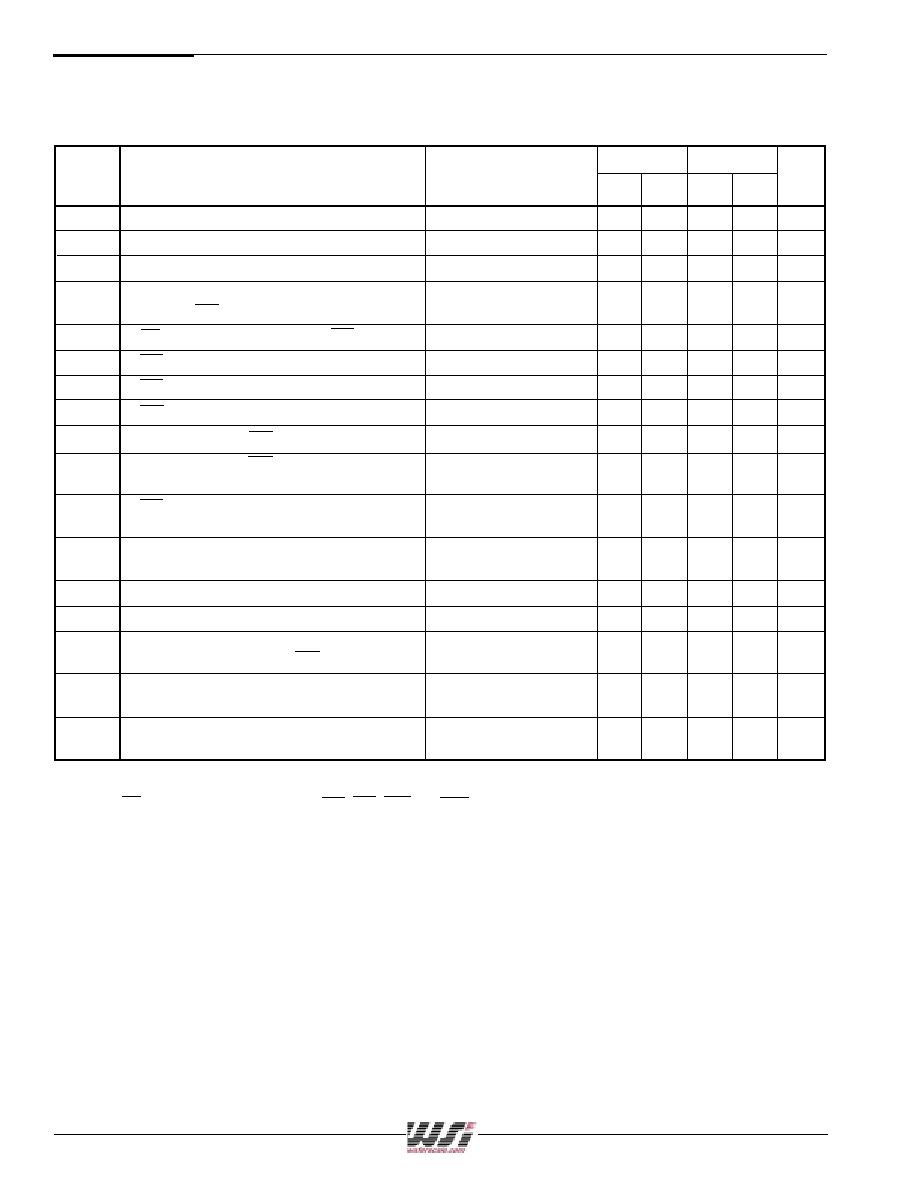
PSD813F Family
Preliminary
100
-15
-20
Symbol
Parameter
Conditions
Min
Max
Min
Max
Unit
tLVLX
ALE or AS Pulse Width
28
30
tAVLX
Address Setup Time
(Note 1)
10
12
ns
tLXAX
Address Hold Time
(Note 1)
12
14
ns
tAVWL
Address Valid to Leading
Edge of WR
(Notes 1 and 3)
30
35
ns
t SLWL
CS Valid to Leading Edge of WR
(Note 3)
34
40
ns
t DVWH
WR Data Setup Time
(Note 3)
45
50
ns
t WHDX
WR Data Hold Time
(Note 3)
8
10
ns
t WLWH
WR Pulse Width
(Note 3)
48
53
ns
tWHAX
Trailing Edge of WR to Address Invalid
(Note 3)
0
ns
tWHPV
Trailing Edge of WR to Port Output
Valid Using I/O Port Data Register
(Note 3)
45
50
ns
tWLMV
WR Valid to Port Output Valid Using
Micro
Cell Register Preset/Clear
(Notes 3 and 4)
90
100
ns
tWHQV1
Byte Programming Operation
Also including
pre-programming time
14
s
tWHQV2
Sector Erase Operation
Note 100% tested
2.2
sec
tQ7VQV
Q7 Valid to Output Valid (Data Polling)
70
75
ns
tVCS
VCC Setup Time
VCC High to First Flash WR Low
45
50
s
tDVMV
Data Valid to Port Output Valid
Using Micro
Cell Register Preset/Clear
(Notes 3 and 5)
90
100
ns
tAVPV
Address Input Valid to Address
(Note 2)
48
55
ns
Output Delay
Write, Erase and Program Timing (3.0 V to 3.6 V Versions)
NOTES: 1. Any input used to select an internal PSD813F function.
2. In multiplexed mode, latched addresses generated from ADIO delay to address output on any Port.
3. WR timing has the same timing as E, LDS, UDS, WRL, and WRH signals.
4. Assuming data is stable before active write signal.
5. Assuming write is active before data becomes valid.
Microcontroller Interface – ZPSD813FV AC/DC Parameters
(3.0 V to 3.6 V Versions)
相关PDF资料 |
PDF描述 |
|---|---|
| ZDVG10A | 7 SEG NUMERIC DISPLAY, GREEN, 10.16 mm |
| ZMG75W | SINGLE COLOR LED, GREEN, 2.3 mm |
| ZMGUY62M-01 | DUAL COLOR LED |
| Z505 | INTERCONNECTION DEVICE |
| Z410 | INTERCONNECTION DEVICE |
相关代理商/技术参数 |
参数描述 |
|---|---|
| ZPSD813F3V-A-15J | 制造商:WSI 功能描述: |
| ZPSD813F4-12JI | 制造商:WSI 功能描述: |
| ZPSD813F4-15J | 制造商:WSI 功能描述: 制造商:STMicroelectronics 功能描述:microcontroller peripheral devices 制造商:STMicroelectronics 功能描述:Flash in-system programmable microcontroller peripheral device |
| ZPSD813F4-90J | 制造商:WSI 功能描述: |
| ZPSD813F5-15J | 制造商:WSI 功能描述: |
发布紧急采购,3分钟左右您将得到回复。