- 您现在的位置:买卖IC网 > PDF目录278507 > ZPSD813F3V-20J 1M X 1 FLASH, 27 I/O, PIA-GENERAL PURPOSE, PQCC52 PDF资料下载
参数资料
| 型号: | ZPSD813F3V-20J |
| 元件分类: | 微控制器/微处理器 |
| 英文描述: | 1M X 1 FLASH, 27 I/O, PIA-GENERAL PURPOSE, PQCC52 |
| 封装: | PLASTIC, LDCC-52 |
| 文件页数: | 73/132页 |
| 文件大小: | 513K |
| 代理商: | ZPSD813F3V-20J |
第1页第2页第3页第4页第5页第6页第7页第8页第9页第10页第11页第12页第13页第14页第15页第16页第17页第18页第19页第20页第21页第22页第23页第24页第25页第26页第27页第28页第29页第30页第31页第32页第33页第34页第35页第36页第37页第38页第39页第40页第41页第42页第43页第44页第45页第46页第47页第48页第49页第50页第51页第52页第53页第54页第55页第56页第57页第58页第59页第60页第61页第62页第63页第64页第65页第66页第67页第68页第69页第70页第71页第72页当前第73页第74页第75页第76页第77页第78页第79页第80页第81页第82页第83页第84页第85页第86页第87页第88页第89页第90页第91页第92页第93页第94页第95页第96页第97页第98页第99页第100页第101页第102页第103页第104页第105页第106页第107页第108页第109页第110页第111页第112页第113页第114页第115页第116页第117页第118页第119页第120页第121页第122页第123页第124页第125页第126页第127页第128页第129页第130页第131页第132页
Preliminary
PSD813F Family
41
The
PSD813F
Functional
Blocks
(cont.)
9.2.2.1 Output Micro
Cell
Eight of the Output Micro
Cells are connected to Ports A and B pins and are named as
McellAB0-7. The other eight Micro
Cells are connected to Ports B and C pins and are
named as McellBC0-7. If an McellAB output is not assigned to a specific pin in PSDabel,
the Micro
Cell Allocator will assign it to either Port A or B. The same is true for a McellBC
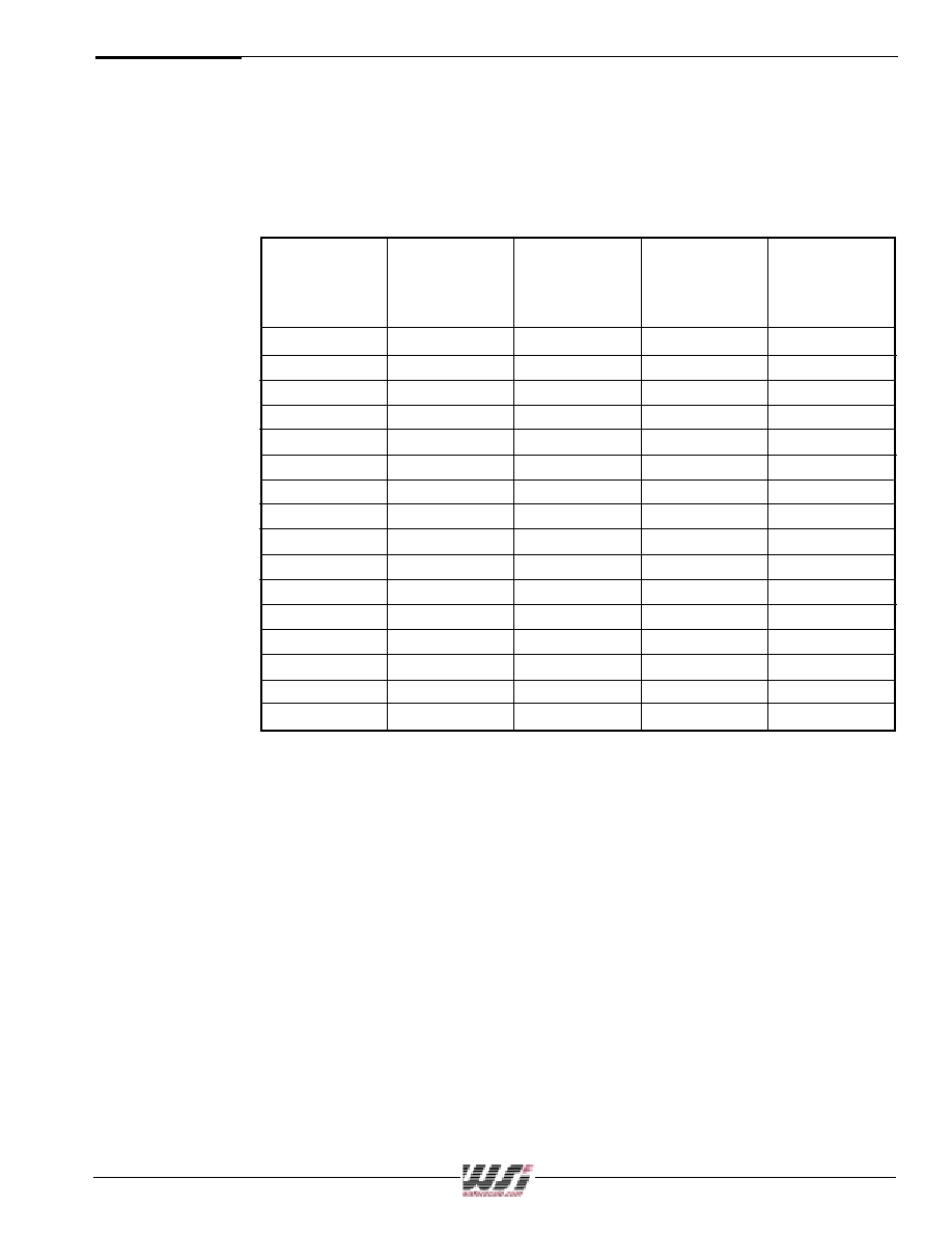
output on Port B or C. Table 16 shows the Micro
Cells and Port assignment.
Maximum
Native
Borrowed
Data Bit for
Output
Port
Product
Loading or
Micro
Cell
Assignment
Terms
Reading
McellAB0
Port A0, B0
3
6
D0
McellAB1
Port A1, B1
3
6
D1
McellAB2
Port A2, B2
3
6
D2
McellAB3
Port A3, B3
3
6
D3
McellAB4
Port A4, B4
3
6
D4
McellAB5
Port A5, B5
3
6
D5
McellAB6
Port A6, B6
3
6
D6
McellAB7
Port A7, B7
3
6
D7
McellBC0
Port B0, C0
4
5
D0
McellBC1
Port B1, C1
4
5
D1
McellBC2
Port B2, C2
4
5
D2
McellBC3
Port B3, C3
4
5
D3
McellBC4
Port B4, C4
4
6
D4
McellBC5
Port B5, C5
4
6
D5
McellBC6
Port B6, C6
4
6
D6
McellBC7
Port B7, C7
4
6
D7
Table 16. Output Micro
Cell Port and Data Bit Assignments
The Output Micro
Cell (OMC) architecture is shown in Figure 15. As shown in the figure,
there are native product terms available from the AND array, and borrowed product terms
available (if unused) from other OMCs. The polarity of the product term is controlled by the
XOR gate. The OMC can implement either sequential logic, using the flip-flop element, or
combinatorial logic. The multiplexer selects between the sequential or combinatorial logic
outputs. The multiplexer output can drive a Port pin and has a feedback path to the AND
array inputs.
The flip-flop in the OMC can be configured as a D, T, JK, or SR type in the PSDabel
program. The flip-flop’s clock, preset, and clear inputs may be driven from a product term
of the AND array. Alternatively, the external CLKIN signal can be used for the clock input to
the flip-flop. The flip-flop is clocked on the rising edge of the clock input. The preset and
clear are active-high inputs. Each clear input can use up to two product terms.
相关PDF资料 |
PDF描述 |
|---|---|
| ZDVG10A | 7 SEG NUMERIC DISPLAY, GREEN, 10.16 mm |
| ZMG75W | SINGLE COLOR LED, GREEN, 2.3 mm |
| ZMGUY62M-01 | DUAL COLOR LED |
| Z505 | INTERCONNECTION DEVICE |
| Z410 | INTERCONNECTION DEVICE |
相关代理商/技术参数 |
参数描述 |
|---|---|
| ZPSD813F3V-A-15J | 制造商:WSI 功能描述: |
| ZPSD813F4-12JI | 制造商:WSI 功能描述: |
| ZPSD813F4-15J | 制造商:WSI 功能描述: 制造商:STMicroelectronics 功能描述:microcontroller peripheral devices 制造商:STMicroelectronics 功能描述:Flash in-system programmable microcontroller peripheral device |
| ZPSD813F4-90J | 制造商:WSI 功能描述: |
| ZPSD813F5-15J | 制造商:WSI 功能描述: |
发布紧急采购,3分钟左右您将得到回复。