- 您现在的位置:买卖IC网 > PDF目录373890 > AD6634 (Analog Devices, Inc.) 80 MSPS, Dual-Channel WCDMA Receive Signal Processor (RSP) PDF资料下载
参数资料
| 型号: | AD6634 |
| 厂商: | Analog Devices, Inc. |
| 元件分类: | 基带处理器 |
| 英文描述: | 80 MSPS, Dual-Channel WCDMA Receive Signal Processor (RSP) |
| 中文描述: | 80 MSPS的双通道的WCDMA接收信号处理器(RSP) |
| 文件页数: | 32/52页 |
| 文件大小: | 925K |
| 代理商: | AD6634 |
第1页第2页第3页第4页第5页第6页第7页第8页第9页第10页第11页第12页第13页第14页第15页第16页第17页第18页第19页第20页第21页第22页第23页第24页第25页第26页第27页第28页第29页第30页第31页当前第32页第33页第34页第35页第36页第37页第38页第39页第40页第41页第42页第43页第44页第45页第46页第47页第48页第49页第50页第51页第52页
REV. 0
–32–
AD6634
5. The Channel BIST located at 0xA7 should be enabled by
setting Bits 19–0 to the number of RCF outputs to observe.
6. Bit 4 of external address register 5 should be set high to
start the soft sync.
7. Set the SYNC bits high for the channels to be tested.
8. Bit 6 must be set to 0 to allow the user to provide test vectors.
The internal pseudo-random number generator may also be
used to generate an input sequence by setting Bit 7 high.
9. An internal full scale sine wave can be inserted when Bit 6
is set to 1 and Bit 7 is cleared.
10. When the SOFT_SYNC is addressed, the selected channels
will come out of the sleep mode and processing will occur.
11. If the user is providing external vectors, the chip may be
brought out of Sleep mode by one of the other methods
provided that either of the IEN inputs is inactive until the
Channel is ready to accept data.
12. After a sufficient amount of time, the Channel BIST Signature
registers 0xA5 and 0xA6 will contain a numeric value that
can be compared to the expected value for a known good
AD6634 with the exact same configuration. If the values
are the same, then there is a very low probability that there
is an error in the channel.
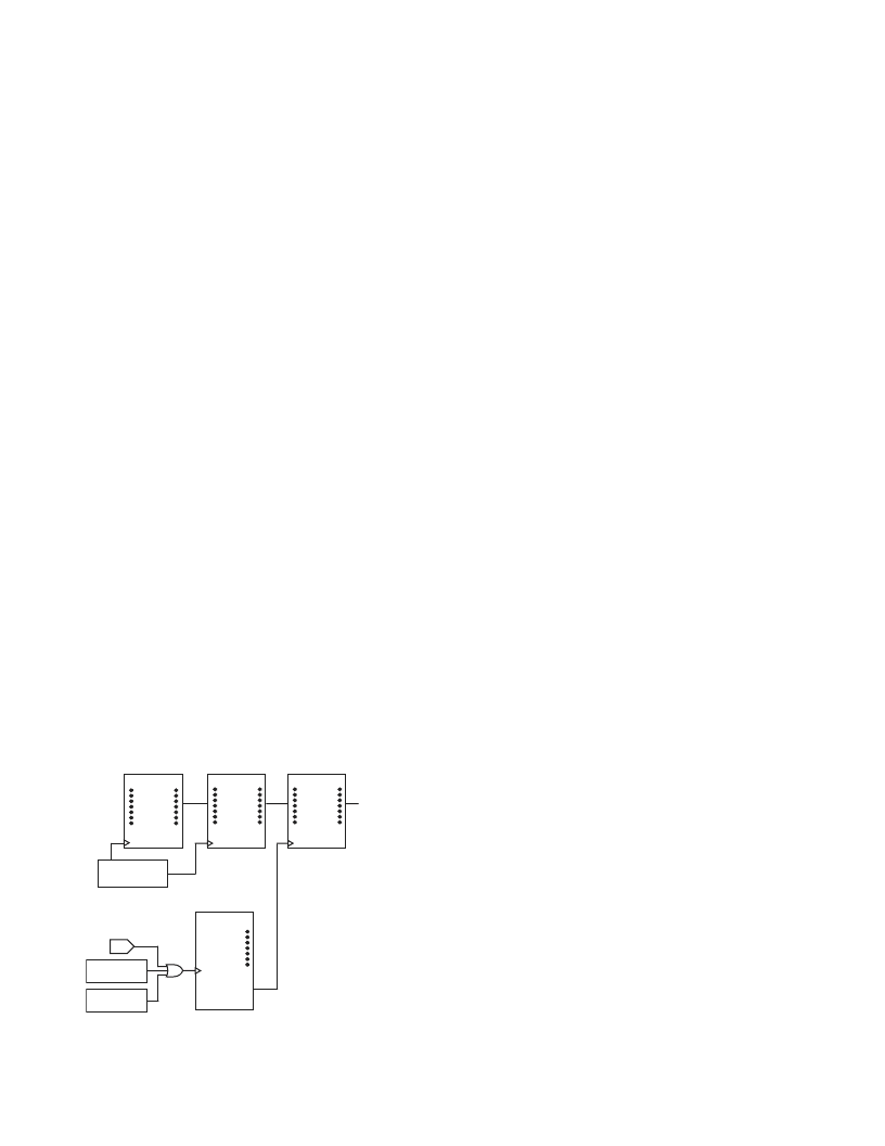
CHIP SYNCHRONIZATION
Two types of synchronization can be achieved with the AD6634.
These are Start and Hop. Each is described in detail below. The
synchronization is accomplished with the use of a shadow register
and a hold-off counter. See Figure 34 for a simplistic schematic of
the NCO Shadow Register and NCO Freq Hold-Off Counter to
understand basic operation. Enabling the clock (AD6634 CLK)
for the hold-off counter can occur with either a Soft_Sync (via the
microport), or a Pin Sync (via any of the four AD6634 SYNC
pins A, B, C, and D). The functions that include shadow registers
to allow synchronization include:
1. Start
2. Hop (NCO Frequency)
I0
I31
Q0
Q31
MICRO
REGISTER
I0
I31
Q0
Q31
SHADOW
REGISTER
I0
I31
Q0
Q31
NCO
FREQUENCY
REGISTER
FROM
MICROPORT
B0
B15
NCO FREQUENCY
UPDATE HOLD OFF
COUNTER
TC
ENB
TO
NCO
SOFT SYNC
ENABLE
AD6634
CLK
PIN SYNC
ENABLE
Figure 34. NCO Shadow Register and Hold-Off Counter
Start
Start refers to the start-up of an individual channel, chip, or
multiple chips. If a channel is not used, it should be put in the
Sleep Mode to reduce power dissipation. Following a hard reset
(low pulse on the AD6634
RESET
pin), all channels are placed
in the Sleep Mode. Channels may also be manually put to sleep
by writing to the mode register controlling the sleep function.
Start with No Sync
If no synchronization is needed to start multiple channels or
multiple AD6634s, the following method should be used to
initialize the device.
1. To program a channel, it must first be set to Sleep Mode (bit
high) (Ext Address 3). All appropriate control and memory
registers (filter) are then loaded. The Start Update Hold-Off
Counter (0x83) should be set to 1.
2. Set the Sleep bits low (Ext Address 3). This enables the channel.
The channel must the Sleep Mode low to activate a channel.
Start with Soft Sync
The AD6634 includes the ability to synchronize channels or
chips under microprocessor control. One action to synchronize
is the start of channels or chips. The Start Update Hold-Off
Counter (0x83) in conjunction with the Start bit and Sync bit
(Ext Address 5) allow this synchronization. Basically, the Start
Update Hold-Off Counter delays the Start of a channel(s) by its
value (number of AD6634 CLKs). The following method is
used to synchronize the start of multiple channels via micropro-
cessor control.
1. Set the appropriate channels to sleep mode (a hard reset to the
AD6634 RESET pin brings all four channels up in sleep mode).
2. Note that the time from when DTACK (Pin 57) goes high
to when the NCO begins processing data is the content of
the Start Update Hold-Off Counter(s) (0x83) + 6 master
clock cycles.
3. Write the Start Update Hold-Off Counter(s) (0x83) to the
appropriate value (greater than 1 and less than 2^16–1). If
the chip(s) is not initialized, all other registers should be
loaded at this step.
4. Write the Start bit and the SYNC bit high (Ext Address 5).
5. This starts the Start Update Hold-Off Counter counting down.
The counter is clocked with the AD6634 CLK signal. When it
reaches a count of 1, the Sleep bit of the appropriate channel(s)
is set low to activate the channel(s).
Start With Pin Sync
The AD6634 has four Sync pins, A, B, C, and D, that can be used
to provide for very accurate synchronization channels. Each
channel can be programmed to look at any of the four sync pins.
Additionally, any or all channels can monitor a single Sync pin or
each can monitor a separate pin, providing complete flexibility of
synchronization. Synchronization of Start with one of the external
signals is accomplished with the following method.
1. Set the appropriate channels to Sleep mode (a hard reset to the
AD6634
RESET
pin brings all four channels up in Sleep mode).
2. Note that the time from when the SYNC pin goes high to when
the NCO begins processing data is the content of the Start
Update Hold-Off Counter(s) (0x83) + 3 master clock cycles.
3. Write the Start Update Hold-Off Counter(s) (0x83) to the
appropriate value (greater than 1 and less than 2
16
–1). If the
chip(s) is not initialized, all other registers should be loaded
at this step.
相关PDF资料 |
PDF描述 |
|---|---|
| AD6634BBC | 80 MSPS, Dual-Channel WCDMA Receive Signal Processor (RSP) |
| AD6634PCB | 80 MSPS, Dual-Channel WCDMA Receive Signal Processor (RSP) |
| AD6635 | 4-Channel, 80 MSPS WCDMA Receive Signal Processor (RSP) |
| AD6635BB | 4-Channel, 80 MSPS WCDMA Receive Signal Processor (RSP) |
| AD6636 | 150 MSPS Wideband Digital Down-Converter (DDC) |
相关代理商/技术参数 |
参数描述 |
|---|---|
| AD6634BBC | 功能描述:IC RSP 80MSPS DUAL 196-CSPBGA RoHS:否 类别:RF/IF 和 RFID >> RF 混频器 系列:AD6634 产品培训模块:Lead (SnPb) Finish for COTS Obsolescence Mitigation Program 标准包装:100 系列:- RF 型:W-CDMA 频率:2.11GHz ~ 2.17GHz 混频器数目:1 增益:17dB 噪音数据:2.2dB 次要属性:- 电流 - 电源:11.7mA 电源电压:2.7 V ~ 3.3 V 包装:托盘 封装/外壳:12-VFQFN 裸露焊盘 供应商设备封装:12-QFN-EP(3x3) |
| AD6634BBCZ | 功能描述:IC RSP 80MSPS DUAL 196CSPBGA RoHS:是 类别:RF/IF 和 RFID >> RF 混频器 系列:AD6634 产品培训模块:Lead (SnPb) Finish for COTS Obsolescence Mitigation Program 标准包装:100 系列:- RF 型:W-CDMA 频率:2.11GHz ~ 2.17GHz 混频器数目:1 增益:17dB 噪音数据:2.2dB 次要属性:- 电流 - 电源:11.7mA 电源电压:2.7 V ~ 3.3 V 包装:托盘 封装/外壳:12-VFQFN 裸露焊盘 供应商设备封装:12-QFN-EP(3x3) |
| AD6634BC/PCB | 制造商:Analog Devices 功能描述:WCDMA RECEIVE SGNL PROCESSOR - Bulk |
| AD6634PCB | 制造商:AD 制造商全称:Analog Devices 功能描述:80 MSPS, Dual-Channel WCDMA Receive Signal Processor (RSP) |
| AD6635 | 制造商:AD 制造商全称:Analog Devices 功能描述:4-Channel, 80 MSPS WCDMA Receive Signal Processor (RSP) |
发布紧急采购,3分钟左右您将得到回复。