- 您现在的位置:买卖IC网 > PDF目录373890 > AD6634 (Analog Devices, Inc.) 80 MSPS, Dual-Channel WCDMA Receive Signal Processor (RSP) PDF资料下载
参数资料
| 型号: | AD6634 |
| 厂商: | Analog Devices, Inc. |
| 元件分类: | 基带处理器 |
| 英文描述: | 80 MSPS, Dual-Channel WCDMA Receive Signal Processor (RSP) |
| 中文描述: | 80 MSPS的双通道的WCDMA接收信号处理器(RSP) |
| 文件页数: | 34/52页 |
| 文件大小: | 925K |
| 代理商: | AD6634 |
第1页第2页第3页第4页第5页第6页第7页第8页第9页第10页第11页第12页第13页第14页第15页第16页第17页第18页第19页第20页第21页第22页第23页第24页第25页第26页第27页第28页第29页第30页第31页第32页第33页当前第34页第35页第36页第37页第38页第39页第40页第41页第42页第43页第44页第45页第46页第47页第48页第49页第50页第51页第52页
REV. 0
–34–
AD6634
PCLK
PxREQ
Px[15:0]
PxACK
PxlQ
PxCH[1:0]
PxCH[1:0] = CHANNEL #
I[15:0]
Q[15:0]
t
DPREQ
t
DPCH
t
DPIQ
t
DPP
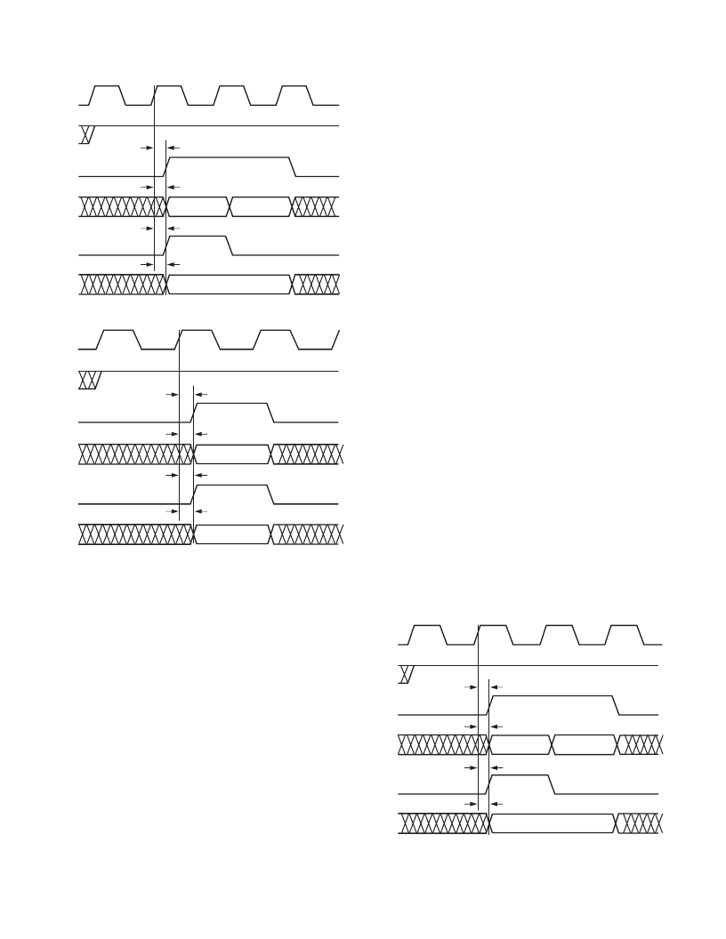
Figure 36. Channel Mode Interleaved Format
PCLK
PxREQ
Px[15:0]
PxACK
PxlQ
PxCH[1:0]
PxCH[1:0] =
CHANNEL #
I[15:8]; Q[7:0]
t
DPREQ
t
DPCH
t
DPIQ
t
DPP
Figure 37. Channel Mode 8I/8Q Parallel Format
The 16-bit interleaved format provides I and Q data for each
output sample on back-to-back PCLK cycles. Both I and Q
words consist of the full port width of 16 bits. Data output is
triggered on the rising edge of PCLK when both REQ and ACK
are asserted. I data is output during the first PCLK cycle; and the
PAIQ and PBIQ output indicator pins are set high to indicate
that I data is on the bus. Q data is output during the subsequent
PCLK cycle; and the PAIQ and PBIQ output indicator pins are
low during this cycle.
The 8-bit concurrent format provides eight bits of I data and
eight bits of Q data simultaneously during one PCLK cycle, also
triggered on the rising edge of PCLK. The I byte occupies the
most significant byte of the port, while the Q byte occupies the
least significant byte. The PAIQ and PBIQ output indicator
pins are set high during the PCLK cycle. Note that if data from
multiple channels are output consecutively, the PAIQ and PBIQ
output indicator pins will remain high until data from all channels
has been output.
The PACH[1:0] and PBCH[1:0] pins provide a 2-bit binary value
indicating the source channel of the data currently being output.
Care should be taken to read data from the port as soon as possible.
If not, the sample will be overwritten when the next new data
sample arrives. This occurs on a per-channel basis; i.e., a
channel 0 sample will only be overwritten by a new channel 0
sample, and so on.
The order of data output is dependent on when data arrived at
the port, which is a function of total decimation rate, Start-Hold-Off
values, and so on. Priority order is, from highest to lowest,
channels 0, 1, 2, 3.
AGC Mode
Parallel port channel mode is selected by clearing Bit 0 of
addresses 0x1A and 0x1C for parallel ports A and B, respectively.
I and Q data output in AGC mode are output from the AGC, not
the individual channels. Each AGC receives data from only two
AD6634 channels; AGC A accepts data from channels 0 and 1,
while AGC B accepts data from channels 2 and 3. Each pair of
channels is required to be configured such that the generation of
output samples from the channels is out of phase (by typically
180 degrees). Each parallel port can provide data from either one
or both AGCs. Bits 1 and 2 of register addresses 0x1A (port A)
and 0x1C (port B) control the inclusion of data from AGCs
A and B, respectively.
AGC mode provides only one I and Q format, which is similar
to the 16-bit interleaved format of Channel mode. When both
REQ and ACK are asserted, the next rising edge of PCLK
triggers the output of a 16-bit AGC I word for one PCLK cycle.
The PAIQ and PBIQ output indicator pins are high during this
cycle, and low otherwise. A 16-bit AGC Q word is provided
during the subsequent PCLK cycle. If the AGC gain word has
been updated since the last sample, a 12-bit RSSI (Receive Signal
Strength Indicator) word is provided during the PCLK cycle
following the Q word on 12 MSBs of the parallel port data pins.
The RSSI word is the bit-inverse of the Signal Gain word used
in the Gain multiplier of the AGC.
The data provided by the PACH[1:0] and PBCH[1:0] pins in
AGC mode is different than that provided in Channel mode. In
AGC mode, PACH[0] and PBCH[0] indicate the AGC source of
the data currently being output (0 = AGC A, 1 = AGC B). PACH[1]
and PBCH[1] indicate whether the current data is an I/Q word or
an AGC RSSI word (0 = I/Q word, 1 = AGC RSSI word). The
two different AGC outputs are shown in Figures 38 and 39.
PCLK
PxREQ
Px[15:0]
PxACK
PxlQ
PxCH[1:0]
I[15:0]
Q[15:0]
PxCH[0] = AGC #
PxCH[1] = 0
t
DPREQ
t
DPCH
t
DPIQ
t
DPP
Figure 38. AGC Output with No RSSI Word
相关PDF资料 |
PDF描述 |
|---|---|
| AD6634BBC | 80 MSPS, Dual-Channel WCDMA Receive Signal Processor (RSP) |
| AD6634PCB | 80 MSPS, Dual-Channel WCDMA Receive Signal Processor (RSP) |
| AD6635 | 4-Channel, 80 MSPS WCDMA Receive Signal Processor (RSP) |
| AD6635BB | 4-Channel, 80 MSPS WCDMA Receive Signal Processor (RSP) |
| AD6636 | 150 MSPS Wideband Digital Down-Converter (DDC) |
相关代理商/技术参数 |
参数描述 |
|---|---|
| AD6634BBC | 功能描述:IC RSP 80MSPS DUAL 196-CSPBGA RoHS:否 类别:RF/IF 和 RFID >> RF 混频器 系列:AD6634 产品培训模块:Lead (SnPb) Finish for COTS Obsolescence Mitigation Program 标准包装:100 系列:- RF 型:W-CDMA 频率:2.11GHz ~ 2.17GHz 混频器数目:1 增益:17dB 噪音数据:2.2dB 次要属性:- 电流 - 电源:11.7mA 电源电压:2.7 V ~ 3.3 V 包装:托盘 封装/外壳:12-VFQFN 裸露焊盘 供应商设备封装:12-QFN-EP(3x3) |
| AD6634BBCZ | 功能描述:IC RSP 80MSPS DUAL 196CSPBGA RoHS:是 类别:RF/IF 和 RFID >> RF 混频器 系列:AD6634 产品培训模块:Lead (SnPb) Finish for COTS Obsolescence Mitigation Program 标准包装:100 系列:- RF 型:W-CDMA 频率:2.11GHz ~ 2.17GHz 混频器数目:1 增益:17dB 噪音数据:2.2dB 次要属性:- 电流 - 电源:11.7mA 电源电压:2.7 V ~ 3.3 V 包装:托盘 封装/外壳:12-VFQFN 裸露焊盘 供应商设备封装:12-QFN-EP(3x3) |
| AD6634BC/PCB | 制造商:Analog Devices 功能描述:WCDMA RECEIVE SGNL PROCESSOR - Bulk |
| AD6634PCB | 制造商:AD 制造商全称:Analog Devices 功能描述:80 MSPS, Dual-Channel WCDMA Receive Signal Processor (RSP) |
| AD6635 | 制造商:AD 制造商全称:Analog Devices 功能描述:4-Channel, 80 MSPS WCDMA Receive Signal Processor (RSP) |
发布紧急采购,3分钟左右您将得到回复。