- 您现在的位置:买卖IC网 > PDF目录9158 > AD9517-3ABCPZ (Analog Devices Inc)IC CLOCK GEN 2.0GHZ VCO 48LFCSP PDF资料下载
参数资料
| 型号: | AD9517-3ABCPZ |
| 厂商: | Analog Devices Inc |
| 文件页数: | 35/80页 |
| 文件大小: | 0K |
| 描述: | IC CLOCK GEN 2.0GHZ VCO 48LFCSP |
| 标准包装: | 1 |
| 类型: | 时钟发生器,扇出配送 |
| PLL: | 是 |
| 输入: | CMOS,LVDS,LVPECL |
| 输出: | CMOS,LVDS,LVPECL |
| 电路数: | 1 |
| 比率 - 输入:输出: | 1:12 |
| 差分 - 输入:输出: | 是/是 |
| 频率 - 最大: | 2.25GHz |
| 除法器/乘法器: | 是/无 |
| 电源电压: | 3.135 V ~ 3.465 V |
| 工作温度: | -40°C ~ 85°C |
| 安装类型: | 表面贴装 |
| 封装/外壳: | 48-VFQFN 裸露焊盘,CSP |
| 供应商设备封装: | 48-LFCSP-VQ(7x7) |
| 包装: | 托盘 |
第1页第2页第3页第4页第5页第6页第7页第8页第9页第10页第11页第12页第13页第14页第15页第16页第17页第18页第19页第20页第21页第22页第23页第24页第25页第26页第27页第28页第29页第30页第31页第32页第33页第34页当前第35页第36页第37页第38页第39页第40页第41页第42页第43页第44页第45页第46页第47页第48页第49页第50页第51页第52页第53页第54页第55页第56页第57页第58页第59页第60页第61页第62页第63页第64页第65页第66页第67页第68页第69页第70页第71页第72页第73页第74页第75页第76页第77页第78页第79页第80页
AD9517-3
Data Sheet
Rev. E | Page 40 of 80
PROGRAMMABLE
N DELAY
REFIN (REF1)
REFIN (REF2)
CLK
REF1
REF2
STATUS
R
DIVIDER
VCO STATUS
PROGRAMMABLE
R DELAY
REFERENCE
SWITCHOVER
REF_SEL
CPRSET VCP
VS
GND
RSET
DISTRIBUTION
REFERENCE
REFMON
CP
STATUS
LD
P, P + 1
PRESCALER
A/B
COUNTERS
N DIVIDER
BYPASS
LF
LOW DROPOUT
REGULATOR (LDO)
VCO
PHASE
FREQUENCY
DETECTOR
LOCK
DETECT
CHARGE
PUMP
PL
L
RE
F
E
RE
NCE
HOLD
0
1
0
1
DIVIDE BY
2, 3, 4, 5, OR 6
06
427-
0
70
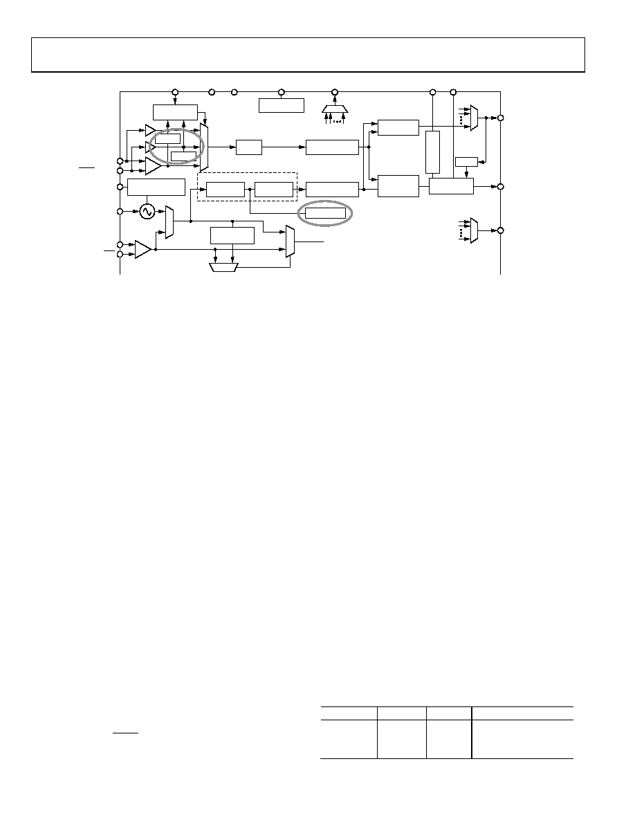
Figure 54. Reference and VCO Status Monitors
VCO Calibration
The AD9517 on-chip VCO must be calibrated to ensure proper
operation over process and temperature. VCO calibration centers
the dc voltage at the internal VCO input (at the LF pin) for the
selected configuration; this is normally required only during initial
configuration and any time the PLL settings change. VCO calibra-
tion is controlled by a calibration controller driven by the R divider
output. The calibration requires that the input reference clock be
present at the REFIN pins, and that the PLL be set up properly to
lock the PLL loop. During the first initialization after a power-up
or a reset of the AD9517, a VCO calibration sequence is initiated
by setting Register 0x018[0] = 1b. This can be done during initial
setup, before executing an update registers (Register 0x232[0] =
1b). Subsequent to initial setup, a VCO calibration sequence is
initiated by resetting Register 0x018[0] = 0b, executing an update
registers operation, setting Register 0x018[0] = 1b, and executing
another update registers operation. A readback bit, Bit 6 in
Register 0x1F, indicates when a VCO calibration is finished
by returning a logic true (that is, 1b).
The sequence of operations for the VCO calibration is as follows:
1.
Program the PLL registers to the proper values for the PLL
loop. Note that that automatic holdover mode must be
disabled, and the VCO divider must not be set to “Static.”
2.
Ensure that the input reference signal is present.
3.
For the initial setting of the registers after a power-up or reset,
initiate VCO calibration by setting Register 0x018[0] = 1b.
Subsequently, whenever a calibration is desired, set
Register 0x018[0] = 0b, update registers; and then set
Register 0x018[0] = 1b, update registers.
4.
A sync operation is initiated internally, causing the outputs
to go to a static state determined by normal sync function
operation.
5.
The VCO calibrates to the desired setting for the requested
VCO frequency.
6.
Internally, the SYNC signal is released, allowing outputs to
continue clocking.
7.
The PLL loop is closed.
8.
The PLL locks.
A sync is executed during the VCO calibration; therefore, the
outputs of the AD9517 are held static during the calibration,
which prevents unwanted frequencies from being produced.
However, at the end of a VCO calibration, the outputs may
resume clocking before the PLL loop is completely settled.
The VCO calibration clock divider is set as shown in Table 54
(Register 0x018[2:1]).
The calibration divider divides the PFD frequency (reference
frequency divided by R) down to the calibration clock. The
calibration occurs at the PFD frequency divided by the
calibration divider setting. Lower VCO calibration clock
frequencies result in longer times for a calibration to be
completed.
The VCO calibration clock frequency is given by
fCAL_CLOCK = fREFIN/(R × cal_div)
where:
fREFIN is the frequency of the REFIN signal.
R is the value of the R divider.
cal_div is the division set for the VCO calibration divider
(Register 0x018[2:1]).
The VCO calibration takes 4400 calibration clock cycles.
Therefore, the VCO calibration time in PLL reference clock
cycles is given by
Time to Calibrate VCO =
4400 × R × cal_div PLL Reference Clock Cycles
Table 29. Example Time to Complete a VCO Calibration
with Different fREFIN Frequencies
fREFIN (MHz)
R Divider
PFD
Time to Calibrate VCO
100
1
100 MHz
88 μs
10
1 MHz
8.8 ms
10
100
100 kHz
88 ms
相关PDF资料 |
PDF描述 |
|---|---|
| AD9517-1ABCPZ | IC CLOCK GEN 2.5GHZ VCO 48LFCSP |
| V110A48H300BL2 | CONVERTER MOD DC/DC 48V 300W |
| AD9511BCPZ | IC CLOCK DIST 5OUT PLL 48LFCSP |
| V110A48H300BL | CONVERTER MOD DC/DC 48V 300W |
| VI-B60-MV | CONVERTER MOD DC/DC 5V 150W |
相关代理商/技术参数 |
参数描述 |
|---|---|
| AD9517-3ABCPZ | 制造商:Analog Devices 功能描述:CLOCK GENERATOR 2.25GHZ LFCSP-48 制造商:Analog Devices 功能描述:CLOCK GENERATOR, 2.25GHZ, LFCSP-48 |
| AD9517-3ABCPZ-RL7 | 功能描述:IC CLOCK GEN 2.0GHZ VCO 48LFCSP RoHS:是 类别:集成电路 (IC) >> 时钟/计时 - 时钟发生器,PLL,频率合成器 系列:- 标准包装:2,000 系列:- 类型:PLL 时钟发生器 PLL:带旁路 输入:LVCMOS,LVPECL 输出:LVCMOS 电路数:1 比率 - 输入:输出:2:11 差分 - 输入:输出:是/无 频率 - 最大:240MHz 除法器/乘法器:是/无 电源电压:3.135 V ~ 3.465 V 工作温度:0°C ~ 70°C 安装类型:表面贴装 封装/外壳:32-LQFP 供应商设备封装:32-TQFP(7x7) 包装:带卷 (TR) |
| AD9517-3BCPZ | 制造商:Analog Devices 功能描述: |
| AD9517-3BCPZ-REEL7 | 制造商:Analog Devices 功能描述: |
| AD9517-3BCPZ-TR | 制造商:Analog Devices 功能描述:12-OUTPUT CLOCK GENERATOR WITH INTEGRATED 2.0 GHZ VCO - Tape and Reel |
发布紧急采购,3分钟左右您将得到回复。