- 您现在的位置:买卖IC网 > PDF目录9158 > AD9517-3ABCPZ (Analog Devices Inc)IC CLOCK GEN 2.0GHZ VCO 48LFCSP PDF资料下载
参数资料
| 型号: | AD9517-3ABCPZ |
| 厂商: | Analog Devices Inc |
| 文件页数: | 38/80页 |
| 文件大小: | 0K |
| 描述: | IC CLOCK GEN 2.0GHZ VCO 48LFCSP |
| 标准包装: | 1 |
| 类型: | 时钟发生器,扇出配送 |
| PLL: | 是 |
| 输入: | CMOS,LVDS,LVPECL |
| 输出: | CMOS,LVDS,LVPECL |
| 电路数: | 1 |
| 比率 - 输入:输出: | 1:12 |
| 差分 - 输入:输出: | 是/是 |
| 频率 - 最大: | 2.25GHz |
| 除法器/乘法器: | 是/无 |
| 电源电压: | 3.135 V ~ 3.465 V |
| 工作温度: | -40°C ~ 85°C |
| 安装类型: | 表面贴装 |
| 封装/外壳: | 48-VFQFN 裸露焊盘,CSP |
| 供应商设备封装: | 48-LFCSP-VQ(7x7) |
| 包装: | 托盘 |
第1页第2页第3页第4页第5页第6页第7页第8页第9页第10页第11页第12页第13页第14页第15页第16页第17页第18页第19页第20页第21页第22页第23页第24页第25页第26页第27页第28页第29页第30页第31页第32页第33页第34页第35页第36页第37页当前第38页第39页第40页第41页第42页第43页第44页第45页第46页第47页第48页第49页第50页第51页第52页第53页第54页第55页第56页第57页第58页第59页第60页第61页第62页第63页第64页第65页第66页第67页第68页第69页第70页第71页第72页第73页第74页第75页第76页第77页第78页第79页第80页
Data Sheet
AD9517-3
Rev. E | Page 43 of 80
Duty Cycle and Duty-Cycle Correction (0, 1)
The duty cycle of the clock signal at the output of a channel is a
result of some or all of the following conditions:
What are the M and N values for the channel?
Is the DCC enabled?
Is the VCO divider used?
What is the CLK input duty cycle? (The internal VCO has
a 50% duty cycle.)
The DCC function is enabled by default for each channel divider.
However, the DCC function can be disabled individually for
each channel divider by setting the DCCOFF bit for that channel.
Certain M and N values for a channel divider result in a non-50%
duty cycle. A non-50% duty cycle can also result with an even
division, if M ≠ N. The duty-cycle correction function
automatically corrects non-50% duty cycles at the channel
divider output to 50% duty cycle. Duty-cycle correction
requires the following channel divider conditions:
An even division must be set as M = N.
An odd division must be set as M = N + 1.
When not bypassed or corrected by the DCC function, the duty
cycle of each channel divider output is the numerical value of
(N + 1)/(N + M + 2), expressed as a percentage (%).
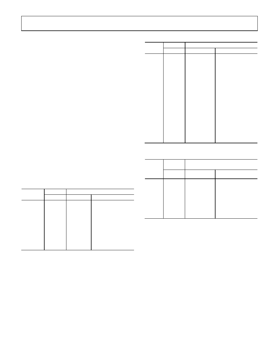
The duty cycle at the output of the channel divider for various
configurations is shown in Table 35 to Table 37.
Table 35. Duty Cycle with VCO Divider; Input Duty Cycle Is 50%
VCO
Divider
DX
Output Duty Cycle
N + M + 2
DCCOFF = 1
DCCOFF = 0
Even
1 (divider
bypassed)
50%
Odd = 3
1 (divider
bypassed)
33.3%
50%
Odd = 5
1 (divider
bypassed)
40%
50%
Even, Odd
Even
(N + 1)/
(N + M + 2)
50%; requires M = N
Even, Odd
Odd
(N + 1)/
(N + M + 2)
50%; requires M = N + 1
Table 36. Duty Cycle with VCO Divider; Input Duty Cycle Is X%
VCO
Divider
DX
Output Duty Cycle
N + M + 2
DCCOFF = 1
DCCOFF = 0
Even
1 (divider
bypassed)
50%
Odd = 3
1 (divider
bypassed)
33.3%
(1 + X%)/3
Odd = 5
1 (divider
bypassed)
40%
(2 + X%)/5
Even
(N + 1)/
(N + M + 2)
50%,
requires M = N
Odd
(N + 1)/
(N + M + 2)
50%,
requires M = N + 1
Odd = 3
Even
(N + 1)/
(N + M + 2)
50%,
requires M = N
Odd = 3
Odd
(N + 1)/
(N + M + 2)
(3N + 4 + X%)/(6N + 9),
requires M = N + 1
Odd = 5
Even
(N + 1)/
(N + M + 2)
50%,
requires M = N
Odd = 5
Odd
(N + 1)/
(N + M + 2)
(5N + 7 + X%)/(10N +
15), requires M = N + 1
Table 37. Channel Divider Output Duty Cycle When the
VCO Divider Is Not Used
Input
Clock
Duty
Cycle
DX
Output Duty Cycle
N + M + 2
DCCOFF = 1
DCCOFF = 0
Any
1
1 (divider
bypassed)
Same as input
duty cycle
Any
Even
(N + 1)/
(M + N + 2)
50%, requires M = N
50%
Odd
(N + 1)/
(M + N + 2)
50%, requires
M = N + 1
X%
Odd
(N + 1)/
(M + N + 2)
(N + 1 + X%)/(2 × N + 3),
requires M = N + 1
The internal VCO has a duty cycle of 50%. Therefore, when the
VCO is connected directly to the output, the duty cycle is 50%.
If the CLK input is routed directly to the output, the duty cycle of
the output is the same as the CLK input.
相关PDF资料 |
PDF描述 |
|---|---|
| AD9517-1ABCPZ | IC CLOCK GEN 2.5GHZ VCO 48LFCSP |
| V110A48H300BL2 | CONVERTER MOD DC/DC 48V 300W |
| AD9511BCPZ | IC CLOCK DIST 5OUT PLL 48LFCSP |
| V110A48H300BL | CONVERTER MOD DC/DC 48V 300W |
| VI-B60-MV | CONVERTER MOD DC/DC 5V 150W |
相关代理商/技术参数 |
参数描述 |
|---|---|
| AD9517-3ABCPZ | 制造商:Analog Devices 功能描述:CLOCK GENERATOR 2.25GHZ LFCSP-48 制造商:Analog Devices 功能描述:CLOCK GENERATOR, 2.25GHZ, LFCSP-48 |
| AD9517-3ABCPZ-RL7 | 功能描述:IC CLOCK GEN 2.0GHZ VCO 48LFCSP RoHS:是 类别:集成电路 (IC) >> 时钟/计时 - 时钟发生器,PLL,频率合成器 系列:- 标准包装:2,000 系列:- 类型:PLL 时钟发生器 PLL:带旁路 输入:LVCMOS,LVPECL 输出:LVCMOS 电路数:1 比率 - 输入:输出:2:11 差分 - 输入:输出:是/无 频率 - 最大:240MHz 除法器/乘法器:是/无 电源电压:3.135 V ~ 3.465 V 工作温度:0°C ~ 70°C 安装类型:表面贴装 封装/外壳:32-LQFP 供应商设备封装:32-TQFP(7x7) 包装:带卷 (TR) |
| AD9517-3BCPZ | 制造商:Analog Devices 功能描述: |
| AD9517-3BCPZ-REEL7 | 制造商:Analog Devices 功能描述: |
| AD9517-3BCPZ-TR | 制造商:Analog Devices 功能描述:12-OUTPUT CLOCK GENERATOR WITH INTEGRATED 2.0 GHZ VCO - Tape and Reel |
发布紧急采购,3分钟左右您将得到回复。