- 您现在的位置:买卖IC网 > PDF目录9158 > AD9517-3ABCPZ (Analog Devices Inc)IC CLOCK GEN 2.0GHZ VCO 48LFCSP PDF资料下载
参数资料
| 型号: | AD9517-3ABCPZ |
| 厂商: | Analog Devices Inc |
| 文件页数: | 76/80页 |
| 文件大小: | 0K |
| 描述: | IC CLOCK GEN 2.0GHZ VCO 48LFCSP |
| 标准包装: | 1 |
| 类型: | 时钟发生器,扇出配送 |
| PLL: | 是 |
| 输入: | CMOS,LVDS,LVPECL |
| 输出: | CMOS,LVDS,LVPECL |
| 电路数: | 1 |
| 比率 - 输入:输出: | 1:12 |
| 差分 - 输入:输出: | 是/是 |
| 频率 - 最大: | 2.25GHz |
| 除法器/乘法器: | 是/无 |
| 电源电压: | 3.135 V ~ 3.465 V |
| 工作温度: | -40°C ~ 85°C |
| 安装类型: | 表面贴装 |
| 封装/外壳: | 48-VFQFN 裸露焊盘,CSP |
| 供应商设备封装: | 48-LFCSP-VQ(7x7) |
| 包装: | 托盘 |
第1页第2页第3页第4页第5页第6页第7页第8页第9页第10页第11页第12页第13页第14页第15页第16页第17页第18页第19页第20页第21页第22页第23页第24页第25页第26页第27页第28页第29页第30页第31页第32页第33页第34页第35页第36页第37页第38页第39页第40页第41页第42页第43页第44页第45页第46页第47页第48页第49页第50页第51页第52页第53页第54页第55页第56页第57页第58页第59页第60页第61页第62页第63页第64页第65页第66页第67页第68页第69页第70页第71页第72页第73页第74页第75页当前第76页第77页第78页第79页第80页
AD9517-3
Data Sheet
Rev. E | Page 78 of 80
CMOS CLOCK DISTRIBUTION
The AD9517 provides four clock outputs (OUT4 to OUT7)
that are selectable as either CMOS or LVDS level outputs.
When selected as CMOS, each output becomes a pair of CMOS
outputs, each of which can be individually turned on or off and
set as noninverting or inverting. These outputs are 3.3 V CMOS
compatible.
Whenever single-ended CMOS clocking is used, some of the
following general guidelines should be used.
Point-to-point nets should be designed such that a driver has
only one receiver on the net, if possible. This allows for simple
termination schemes and minimizes ringing due to possible
mismatched impedances on the net.
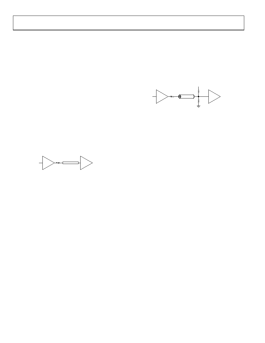
Series termination at the source is generally required to provide
transmission line matching and/or to reduce current transients
at the driver. The value of the resistor is dependent on the board
design and timing requirements (typically 10 to 100 is used).
CMOS outputs are also limited in terms of the capacitive load
or trace length that they can drive. Typically, trace lengths of less
than 3 inches are recommended to preserve signal rise/fall times
and preserve signal integrity.
CMOS
10
60.4
(1.0 INCH)
MICROSTRIP
06427-
076
Figure 75. Series Termination of CMOS Output
Termination at the far end of the PCB trace is a second option.
The CMOS outputs of the AD9517 do not supply enough current
to provide a full voltage swing with a low impedance resistive,
far-end termination, as shown in Figure 76. The far-end
termination network should match the PCB trace impedance and
provide the desired switching point. The reduced signal swing
may still meet receiver input requirements in some applications.
This can be useful when driving long trace lengths on less
critical nets.
CMOS
10
50
100
VS
06427-
077
Figure 76. CMOS Output with Far-End Termination
Because of the limitations of single-ended CMOS clocking,
consider using differential outputs when driving high speed
signals over long traces. The AD9517 offers both LVPECL and
LVDS outputs that are better suited for driving long traces
where the inherent noise immunity of differential signaling
provides superior performance for clocking converters.
相关PDF资料 |
PDF描述 |
|---|---|
| AD9517-1ABCPZ | IC CLOCK GEN 2.5GHZ VCO 48LFCSP |
| V110A48H300BL2 | CONVERTER MOD DC/DC 48V 300W |
| AD9511BCPZ | IC CLOCK DIST 5OUT PLL 48LFCSP |
| V110A48H300BL | CONVERTER MOD DC/DC 48V 300W |
| VI-B60-MV | CONVERTER MOD DC/DC 5V 150W |
相关代理商/技术参数 |
参数描述 |
|---|---|
| AD9517-3ABCPZ | 制造商:Analog Devices 功能描述:CLOCK GENERATOR 2.25GHZ LFCSP-48 制造商:Analog Devices 功能描述:CLOCK GENERATOR, 2.25GHZ, LFCSP-48 |
| AD9517-3ABCPZ-RL7 | 功能描述:IC CLOCK GEN 2.0GHZ VCO 48LFCSP RoHS:是 类别:集成电路 (IC) >> 时钟/计时 - 时钟发生器,PLL,频率合成器 系列:- 标准包装:2,000 系列:- 类型:PLL 时钟发生器 PLL:带旁路 输入:LVCMOS,LVPECL 输出:LVCMOS 电路数:1 比率 - 输入:输出:2:11 差分 - 输入:输出:是/无 频率 - 最大:240MHz 除法器/乘法器:是/无 电源电压:3.135 V ~ 3.465 V 工作温度:0°C ~ 70°C 安装类型:表面贴装 封装/外壳:32-LQFP 供应商设备封装:32-TQFP(7x7) 包装:带卷 (TR) |
| AD9517-3BCPZ | 制造商:Analog Devices 功能描述: |
| AD9517-3BCPZ-REEL7 | 制造商:Analog Devices 功能描述: |
| AD9517-3BCPZ-TR | 制造商:Analog Devices 功能描述:12-OUTPUT CLOCK GENERATOR WITH INTEGRATED 2.0 GHZ VCO - Tape and Reel |
发布紧急采购,3分钟左右您将得到回复。