- 您现在的位置:买卖IC网 > PDF目录9158 > AD9517-3ABCPZ (Analog Devices Inc)IC CLOCK GEN 2.0GHZ VCO 48LFCSP PDF资料下载
参数资料
| 型号: | AD9517-3ABCPZ |
| 厂商: | Analog Devices Inc |
| 文件页数: | 48/80页 |
| 文件大小: | 0K |
| 描述: | IC CLOCK GEN 2.0GHZ VCO 48LFCSP |
| 标准包装: | 1 |
| 类型: | 时钟发生器,扇出配送 |
| PLL: | 是 |
| 输入: | CMOS,LVDS,LVPECL |
| 输出: | CMOS,LVDS,LVPECL |
| 电路数: | 1 |
| 比率 - 输入:输出: | 1:12 |
| 差分 - 输入:输出: | 是/是 |
| 频率 - 最大: | 2.25GHz |
| 除法器/乘法器: | 是/无 |
| 电源电压: | 3.135 V ~ 3.465 V |
| 工作温度: | -40°C ~ 85°C |
| 安装类型: | 表面贴装 |
| 封装/外壳: | 48-VFQFN 裸露焊盘,CSP |
| 供应商设备封装: | 48-LFCSP-VQ(7x7) |
| 包装: | 托盘 |
第1页第2页第3页第4页第5页第6页第7页第8页第9页第10页第11页第12页第13页第14页第15页第16页第17页第18页第19页第20页第21页第22页第23页第24页第25页第26页第27页第28页第29页第30页第31页第32页第33页第34页第35页第36页第37页第38页第39页第40页第41页第42页第43页第44页第45页第46页第47页当前第48页第49页第50页第51页第52页第53页第54页第55页第56页第57页第58页第59页第60页第61页第62页第63页第64页第65页第66页第67页第68页第69页第70页第71页第72页第73页第74页第75页第76页第77页第78页第79页第80页
AD9517-3
Data Sheet
Rev. E | Page 52 of 80
Read
If the instruction word is for a read operation, the next N × 8
SCLK cycles clock out the data from the address specified in the
instruction word, where N is 1 to 3 as determined by [W1:W0].
If N = 4, the read operation is in streaming mode, continuing
until CS is raised. Streaming mode does not skip over reserved
or blank registers. The readback data is valid on the falling
edge of SCLK.
The default mode of the AD9517 serial control port is the
bidirectional mode. In bidirectional mode, both the sent data
and the readback data appear on the SDIO pin. It is also possible to
set the AD9517 to unidirectional mode via the SDO active bit,
Register 0x000[0] = 1b. In unidirectional mode, the readback
data appears on the SDO pin.
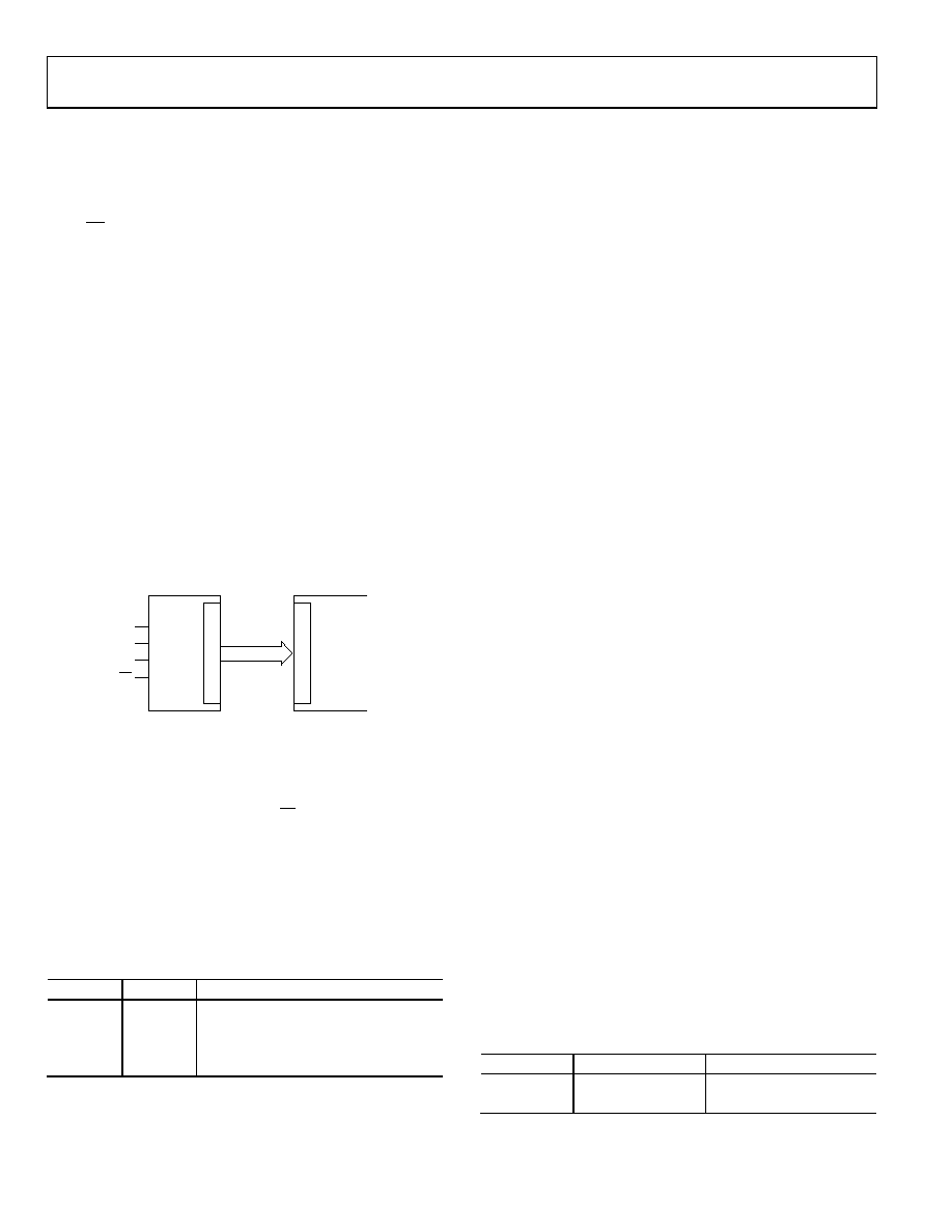
A readback request reads the data that is in the serial control
port buffer area, or the data that is in the active registers (see
Figure 63). Readback of the buffer or active registers is controlled
by Register 0x004[0].
The AD9517 supports only the long instruction mode; therefore,
Register 0x000[4:3] must be set to 11b. (This register uses mirrored
bits.) Long instruction mode is the default at power-up or reset.
The AD9517 uses Register Address 0x000 to Register
Address 0x232.
SCLK
SDIO
SDO
CS
SERIAL
CONTROL
PORT
BUF
F
E
R
RE
G
IS
T
E
RS
UPDATE
REGISTERS
WRITE REGISTER 0x232 = 0x01
TO UDATE REGISTERS
A
C
T
IVE
R
EG
IST
ER
S
06427-
037
Figure 63. Relationship Between Serial Control Port Buffer Registers and
Active Registers of the AD9517
THE INSTRUCTION WORD (16 BITS)
The MSB of the instruction word is R/W, which indicates
whether the instruction is a read or a write. The next two bits,
[W1:W0], indicate the length of the transfer in bytes. The final
13 bits are the address ([A12:A0]) at which to begin the read or
write operation.
For a write, the instruction word is followed by the number of
bytes of data indicated by Bits[W1:W0] (see Table 47).
Table 47. Byte Transfer Count
W1
W0
Bytes to Transfer
0
1
0
1
2
1
0
3
1
Streaming mode
The 13 bits found in [A12:A0] select the address within the
register map that is written to or read from during the data
transfer portion of the communications cycle. Only Bits[A9:A0]
are needed to cover the range of the 0x232 registers used by the
AD9517. Bits[A12:A10] must always be set to 0b. For multibyte
transfers, this address is the starting byte address. In MSB first
mode, subsequent bytes decrement the address.
MSB/LSB FIRST TRANSFERS
The AD9517 instruction word and byte data can be MSB first
or LSB first. Any data written to Register 0x000 must be mirrored;
the upper four bits (Bits[7:4]) with the lower four bits (Bits[3:0).
This makes it irrelevant whether LSB first or MSB first is in
effect. As an example of this mirroring, see the default setting
for this register: 0x18, which mirrors Bit 4 and Bit 3. This sets
the long instruction mode (which is the default and the only
mode that is supported).
The default for the AD9517 is MSB first.
When LSB first is set by Register 0x000[1] and Register 0x000[6],
it takes effect immediately because it affects only the operation
of the serial control port and does not require that an update be
executed.
When MSB first mode is active, the instruction and data bytes
must be written from MSB to LSB. Multibyte data transfers in
MSB first format start with an instruction byte that includes the
register address of the most significant data byte. Subsequent
data bytes must follow in order from the high address to the low
address. In MSB first mode, the serial control port internal
address generator decrements for each data byte of the
multibyte transfer cycle.
When LSB first is active, the instruction and data bytes must be
written from LSB to MSB. Multibyte data transfers in LSB first
format start with an instruction byte that includes the register
address of the least significant data byte followed by multiple
data bytes. The internal byte address generator of the serial
control port increments for each byte of the multibyte
transfer cycle.
The AD9517 serial control port register address decrements
from the register address just written toward 0x000 for multibyte
I/O operations if the MSB first mode is active (default). If the LSB
first mode is active, the register address of the serial control port
increments from the address just written toward Address 0x232
for multibyte I/O operations.
Streaming mode always terminates when it hits Address 0x232.
Note that unused addresses are not skipped during multibyte
I/O operations.
Table 48. Streaming Mode (No Addresses Are Skipped)
Write Mode
Address Direction
Stop Sequence
LSB first
Increment
0x230, 0x231, 0x232, stop
MSB first
Decrement
0x001, 0x000, 0x232, stop
相关PDF资料 |
PDF描述 |
|---|---|
| AD9517-1ABCPZ | IC CLOCK GEN 2.5GHZ VCO 48LFCSP |
| V110A48H300BL2 | CONVERTER MOD DC/DC 48V 300W |
| AD9511BCPZ | IC CLOCK DIST 5OUT PLL 48LFCSP |
| V110A48H300BL | CONVERTER MOD DC/DC 48V 300W |
| VI-B60-MV | CONVERTER MOD DC/DC 5V 150W |
相关代理商/技术参数 |
参数描述 |
|---|---|
| AD9517-3ABCPZ | 制造商:Analog Devices 功能描述:CLOCK GENERATOR 2.25GHZ LFCSP-48 制造商:Analog Devices 功能描述:CLOCK GENERATOR, 2.25GHZ, LFCSP-48 |
| AD9517-3ABCPZ-RL7 | 功能描述:IC CLOCK GEN 2.0GHZ VCO 48LFCSP RoHS:是 类别:集成电路 (IC) >> 时钟/计时 - 时钟发生器,PLL,频率合成器 系列:- 标准包装:2,000 系列:- 类型:PLL 时钟发生器 PLL:带旁路 输入:LVCMOS,LVPECL 输出:LVCMOS 电路数:1 比率 - 输入:输出:2:11 差分 - 输入:输出:是/无 频率 - 最大:240MHz 除法器/乘法器:是/无 电源电压:3.135 V ~ 3.465 V 工作温度:0°C ~ 70°C 安装类型:表面贴装 封装/外壳:32-LQFP 供应商设备封装:32-TQFP(7x7) 包装:带卷 (TR) |
| AD9517-3BCPZ | 制造商:Analog Devices 功能描述: |
| AD9517-3BCPZ-REEL7 | 制造商:Analog Devices 功能描述: |
| AD9517-3BCPZ-TR | 制造商:Analog Devices 功能描述:12-OUTPUT CLOCK GENERATOR WITH INTEGRATED 2.0 GHZ VCO - Tape and Reel |
发布紧急采购,3分钟左右您将得到回复。