- 您现在的位置:买卖IC网 > PDF目录10534 > AD9600ABCPZ-105 (Analog Devices Inc)IC ADC 10BIT 105MSPS 64LFCSP PDF资料下载
参数资料
| 型号: | AD9600ABCPZ-105 |
| 厂商: | Analog Devices Inc |
| 文件页数: | 26/72页 |
| 文件大小: | 0K |
| 描述: | IC ADC 10BIT 105MSPS 64LFCSP |
| 标准包装: | 1 |
| 位数: | 10 |
| 采样率(每秒): | 105M |
| 数据接口: | 串行,SPI? |
| 转换器数目: | 2 |
| 功率耗散(最大): | 650mW |
| 电压电源: | 模拟和数字 |
| 工作温度: | -40°C ~ 85°C |
| 安装类型: | 表面贴装 |
| 封装/外壳: | 64-VFQFN 裸露焊盘,CSP |
| 供应商设备封装: | 64-LFCSP-VQ(9x9) |
| 包装: | 托盘 |
| 输入数目和类型: | 4 个单端,单极;2 个差分,单极 |
第1页第2页第3页第4页第5页第6页第7页第8页第9页第10页第11页第12页第13页第14页第15页第16页第17页第18页第19页第20页第21页第22页第23页第24页第25页当前第26页第27页第28页第29页第30页第31页第32页第33页第34页第35页第36页第37页第38页第39页第40页第41页第42页第43页第44页第45页第46页第47页第48页第49页第50页第51页第52页第53页第54页第55页第56页第57页第58页第59页第60页第61页第62页第63页第64页第65页第66页第67页第68页第69页第70页第71页第72页
AD9600
Rev. B | Page 32 of 72
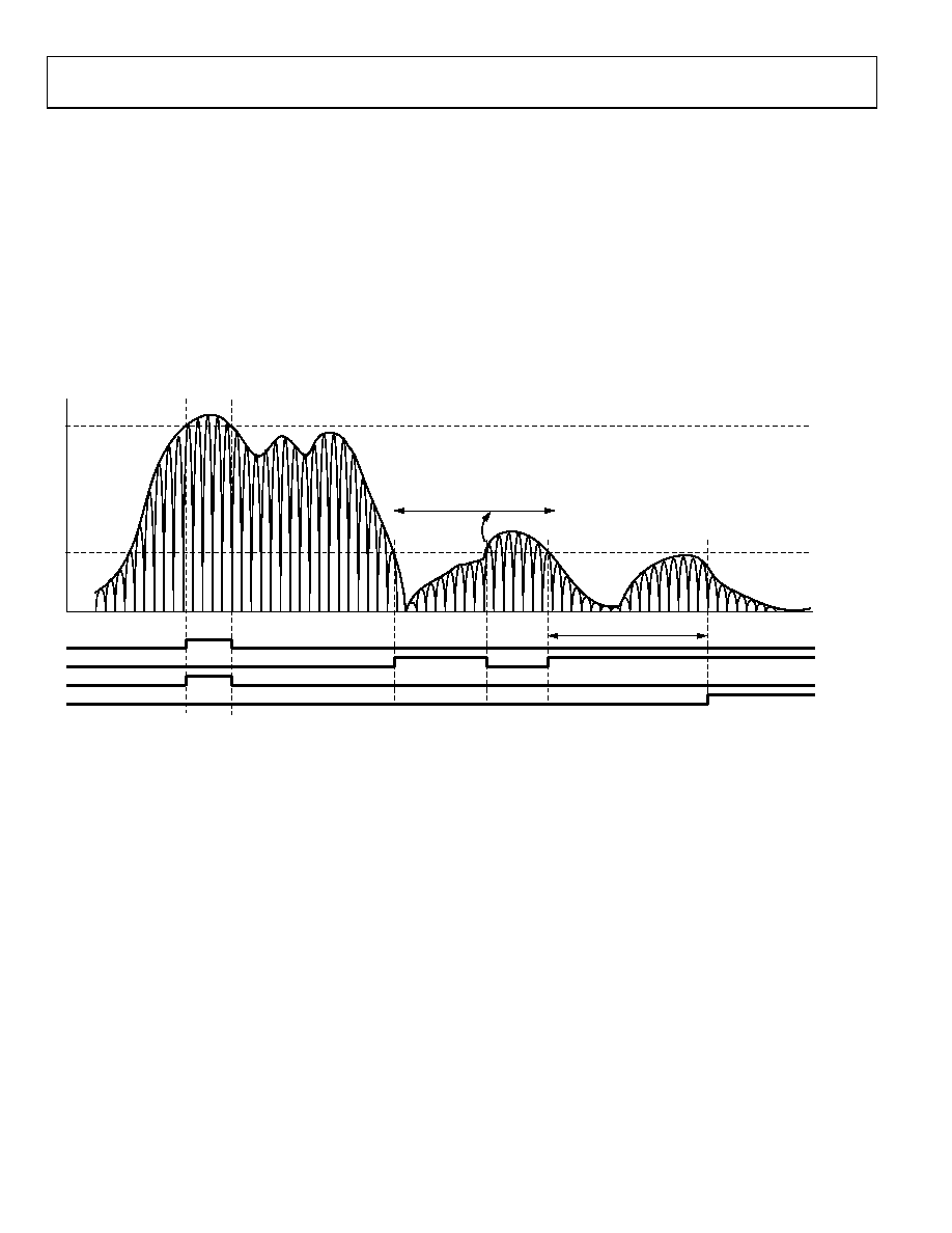
Increment Gain (IG) and Decrement Gain (DG)
The increment gain and decrement gain indicators are intended
to be used together to provide information to enable external gain
control. The decrement gain indicator works in conjunction with
the coarse upper threshold bits, asserting when the input
magnitude is greater than the 3-bit value in the coarse upper
threshold register (Address 0x105). The increment gain indicator,
similarly, corresponds with the fine lower threshold bits, except
that it is asserted only if the input magnitude is less than the
value programmed in the fine lower threshold register after the
dwell time elapses. This dwell time is set by the 16-bit increase
gain dwell time register (Address 0x10A and Address 0x10B) and
is in units of ADC input clock cycles ranging from 1 to 65,535. The
fine lower threshold register is a 13-bit register that is compared
with the magnitude at the output of the ADC. This comparison
is subject to the ADC clock latency but allows a finer, more
accurate comparison. The fine threshold magnitude is defined
in Equation 1 (see the Fine Upper Threshold (F_UT) section).
The decrement gain output is influenced by the fast detect output
pins, which provide a fast indication of potential overrange
conditions. Assertion of the increment gain indicator is based
on the comparison at the output of the ADC, requiring the input
magnitude to remain below an accurate, programmable level for a
predefined period before signaling external circuitry to increase
the gain.
The operation of the IG and DG indicators is shown in Figure 66.
0
69
09
-09
7
UPPER THRESHOLD (COARSE OR FINE)
FINE LOWER THRESHOLD
IG
DG
F_LT
C_UT OR F_UT*
DWELL TIME
TIMER RESET BY
RISE ABOVE F_LT
TIMER COMPLETES BEFORE
SIGNAL RISES ABOVE F_LT
NOTE: OUTPUTS FOLLOW THE INSTANTANEOUS SIGNAL LEVEL AND NOT THE ENVELOPE BUT ARE GUARANTEED ACTIVE FOR A MINIMUM OF TWO ADC CLOCK CYCLES.
*C_UT AND F_UT DIFFER ONLY IN ACCURACY AND LATENCY.
DWELL TIME
Figure 66. Threshold Settings for C_UT, F_UT, F_LT, IG, and DG
相关PDF资料 |
PDF描述 |
|---|---|
| VE-241-IW-F3 | CONVERTER MOD DC/DC 12V 100W |
| AD7653ACPZ | IC ADC 16BIT UNIPOLAR 48LFCSP |
| VE-241-IW-F2 | CONVERTER MOD DC/DC 12V 100W |
| LTC1279CG | IC A/DCONV SAMPLNG W/SHTDN24SSOP |
| VI-BTN-IV-F4 | CONVERTER MOD DC/DC 18.5V 150W |
相关代理商/技术参数 |
参数描述 |
|---|---|
| AD9600ABCPZ-125 | 功能描述:IC ADC 10BIT 125MSPS 64LFCSP RoHS:是 类别:集成电路 (IC) >> 数据采集 - 模数转换器 系列:- 其它有关文件:TSA1204 View All Specifications 标准包装:1 系列:- 位数:12 采样率(每秒):20M 数据接口:并联 转换器数目:2 功率耗散(最大):155mW 电压电源:模拟和数字 工作温度:-40°C ~ 85°C 安装类型:表面贴装 封装/外壳:48-TQFP 供应商设备封装:48-TQFP(7x7) 包装:Digi-Reel® 输入数目和类型:4 个单端,单极;2 个差分,单极 产品目录页面:1156 (CN2011-ZH PDF) 其它名称:497-5435-6 |
| AD9600ABCPZ-150 | 功能描述:IC ADC 10BIT 150MSPS 64LFCSP RoHS:是 类别:集成电路 (IC) >> 数据采集 - 模数转换器 系列:- 标准包装:1 系列:- 位数:14 采样率(每秒):83k 数据接口:串行,并联 转换器数目:1 功率耗散(最大):95mW 电压电源:双 ± 工作温度:0°C ~ 70°C 安装类型:通孔 封装/外壳:28-DIP(0.600",15.24mm) 供应商设备封装:28-PDIP 包装:管件 输入数目和类型:1 个单端,双极 |
| AD9600BCPZ-105 | 制造商:Analog Devices 功能描述:ADC Dual Pipelined 105Msps 10-bit Parallel/LVDS 64-Pin LFCSP EP |
| AD9600BCPZ-125 | 制造商:Analog Devices 功能描述:ADC Dual Pipelined 125Msps 10-bit Parallel/LVDS 64-Pin LFCSP EP |
| AD9600BCPZ-150 | 制造商:Analog Devices 功能描述: |
发布紧急采购,3分钟左右您将得到回复。