- 您现在的位置:买卖IC网 > PDF目录10534 > AD9600ABCPZ-105 (Analog Devices Inc)IC ADC 10BIT 105MSPS 64LFCSP PDF资料下载
参数资料
| 型号: | AD9600ABCPZ-105 |
| 厂商: | Analog Devices Inc |
| 文件页数: | 43/72页 |
| 文件大小: | 0K |
| 描述: | IC ADC 10BIT 105MSPS 64LFCSP |
| 标准包装: | 1 |
| 位数: | 10 |
| 采样率(每秒): | 105M |
| 数据接口: | 串行,SPI? |
| 转换器数目: | 2 |
| 功率耗散(最大): | 650mW |
| 电压电源: | 模拟和数字 |
| 工作温度: | -40°C ~ 85°C |
| 安装类型: | 表面贴装 |
| 封装/外壳: | 64-VFQFN 裸露焊盘,CSP |
| 供应商设备封装: | 64-LFCSP-VQ(9x9) |
| 包装: | 托盘 |
| 输入数目和类型: | 4 个单端,单极;2 个差分,单极 |
第1页第2页第3页第4页第5页第6页第7页第8页第9页第10页第11页第12页第13页第14页第15页第16页第17页第18页第19页第20页第21页第22页第23页第24页第25页第26页第27页第28页第29页第30页第31页第32页第33页第34页第35页第36页第37页第38页第39页第40页第41页第42页当前第43页第44页第45页第46页第47页第48页第49页第50页第51页第52页第53页第54页第55页第56页第57页第58页第59页第60页第61页第62页第63页第64页第65页第66页第67页第68页第69页第70页第71页第72页
AD9600
Rev. B | Page 48 of 72
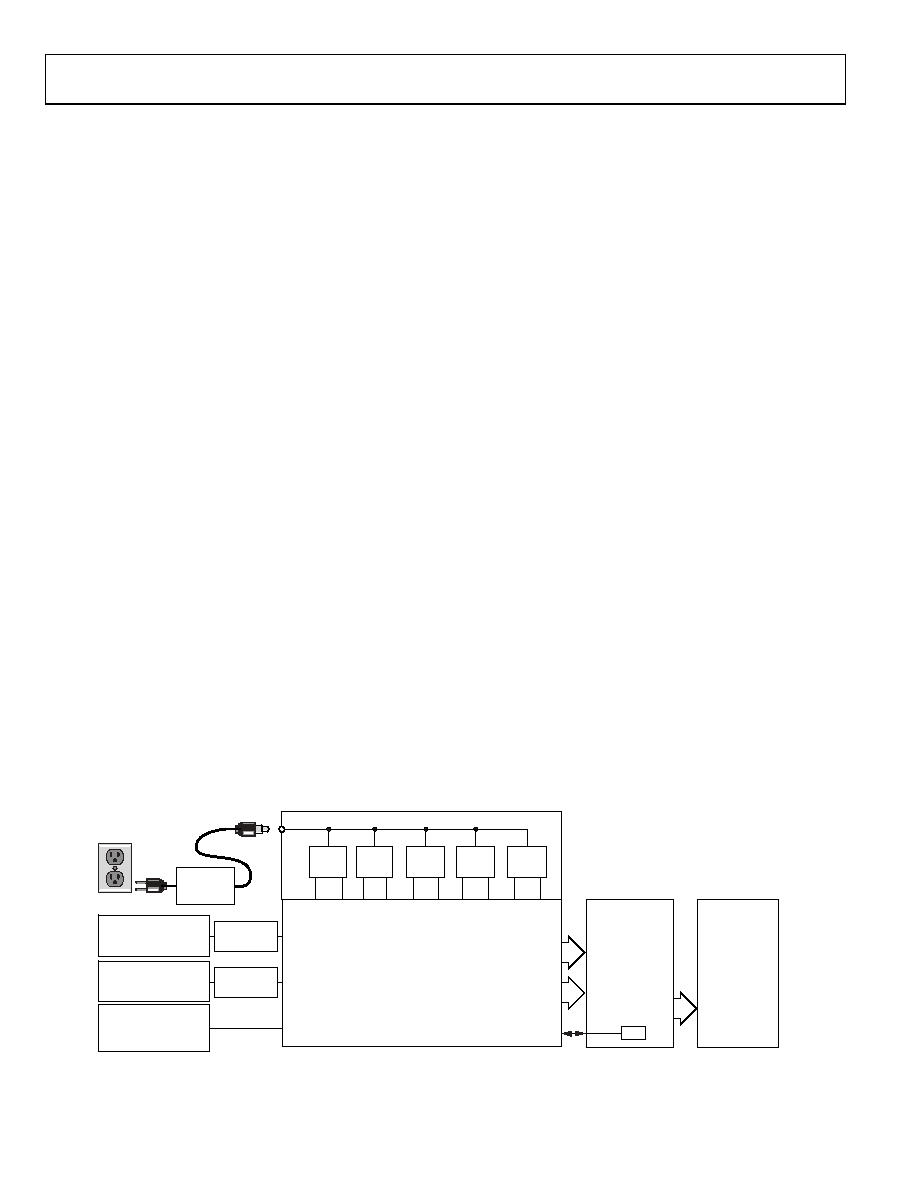
EVALUATION BOARD
The AD9600 evaluation board provides all of the support
circuitry required to operate the ADC in its various modes and
configurations. The converter can be driven differentially using the
double-balun configuration (default) or an AD8352 differential
driver. The ADC can also be driven in a single-ended fashion.
Separate power pins are provided to isolate the DUT from the
AD8352 drive circuitry. Each input configuration can be selected
by properly connecting various components (see Figure 74 to
Figure 83). Figure 73 shows the typical bench characterization
setup used to evaluate the ac performance of the AD9600.
It is critical that the signal sources used for the analog input and
clock have very low phase noise (<<1 ps rms jitter) to realize the
optimum performance of the converter. Proper filtering of the
analog input signal to remove harmonics and lower the integrated
or broadband noise at the input is also necessary to achieve the
specified noise performance.
layout diagrams that demonstrate the routing and grounding
techniques that should be applied at the system level.
POWER SUPPLIES
The evaluation board comes with a wall-mountable switching
power supply that provides a 6 V, 2 A maximum output. Connect
the supply to the rated 100 V ac to 240 V ac wall outlet at 47 Hz
to 63 Hz. The output of the supply is a 2.1 mm inner diameter
circular jack that connects to the PCB at J16. Once on the PC
board, the 6 V supply is fused and conditioned before connecting
to six low dropout linear regulators that supply the proper bias
to each of the various sections of the board.
The evaluation board can be operated using external supplies
by removing L1, L3, L4, and L13 to disconnect the voltage
regulators supplied from the switching power supply. This
enables the user to individually bias each section of the board.
Use P3 and P4 to connect a different supply for each section.
At least one 1.8 V supply is needed with a 1 A current capability
for AVDD and DVDD; a separate 1.8 V to 3.3 V supply is
recommended for DRVDD. To operate the evaluation board
using the AD8352 driver, a separate 5.0 V supply (AMP VDD)
with a 1 A current capability is needed. To operate the evaluation
board using the alternative SPI options, a separate 3.3 V analog
supply (VS) is needed in addition to the other supplies. The
3.3 V supply (VS) should also have a 1 A current capability.
Using Solder Jumper SJ35 allows the user to separate AVDD
and DVDD if desired.
INPUT SIGNALS
When connecting the clock and analog sources to the evaluation
board, use clean signal generators with low phase noise, such as
Rohde & Schwarz SMA100A or Agilent HP8644 signal generators
or the equivalent, as well as a 1 m, shielded, RG-58, 50 Ω coaxial
cable. Enter the desired frequency and amplitude for the ADC.
The AD9600 evaluation board from Analog Devices can accept
a ~2.8 V p-p or a 13 dBm sine wave input for the clock. When
connecting the analog input source, it is recommended to use a
multipole, narrow-band, band-pass filter with 50 Ω terminations.
Good choices of such band-pass filters are available from TTE,
Allen Avionics, and K&L Microwave, Inc. Connect the filter
directly to the evaluation board, if possible.
OUTPUT SIGNALS
The parallel CMOS outputs interface directly with the Analog
Devices standard ADC data capture board (HSC-ADC-
EVALCZ). For more information on the ADC data capture
boards and their optional settings, visit www.analog.com/FIFO.
USB
CONNECTION
AD9600
EVALUATION BOARD
10-BIT
PARALLEL
CMOS
10-BIT
PARALLEL
CMOS
HSC-ADC-EVALCZ
FPGA BASED
DATA
CAPTURE BOARD
PC RUNNING
VISUAL ANALOG
AND SPI
CONTROLLER
SOFTWARE
1.8V
–+
A
V
DD
I
N
VS
DRV
DD
I
N
GN
D
GN
D
–+
5.0V
GN
D
A
M
P
VD
D
3.3V
6V DC
2A MAX
WALL OUTLET
100V AC TO 240V AC
47Hz TO 63Hz
SWITCHING
POWER
SUPPLY
–+
GN
D
3.3V
VC
P
–+
GN
D
3.3V
SPI
06
909
-30
0
ROHDE & SCHWARZ,
SMA100A,
2V p-p SIGNAL
SYNTHESIZER
CLK
ROHDE & SCHWARZ,
SMA100A,
2V p-p SIGNAL
SYNTHESIZER
AINB
BAND-PASS
FILTER
ROHDE & SCHWARZ,
SMA100A,
2V p-p SIGNAL
SYNTHESIZER
AINA
BAND-PASS
FILTER
Figure 73. Evaluation Board Connection
相关PDF资料 |
PDF描述 |
|---|---|
| VE-241-IW-F3 | CONVERTER MOD DC/DC 12V 100W |
| AD7653ACPZ | IC ADC 16BIT UNIPOLAR 48LFCSP |
| VE-241-IW-F2 | CONVERTER MOD DC/DC 12V 100W |
| LTC1279CG | IC A/DCONV SAMPLNG W/SHTDN24SSOP |
| VI-BTN-IV-F4 | CONVERTER MOD DC/DC 18.5V 150W |
相关代理商/技术参数 |
参数描述 |
|---|---|
| AD9600ABCPZ-125 | 功能描述:IC ADC 10BIT 125MSPS 64LFCSP RoHS:是 类别:集成电路 (IC) >> 数据采集 - 模数转换器 系列:- 其它有关文件:TSA1204 View All Specifications 标准包装:1 系列:- 位数:12 采样率(每秒):20M 数据接口:并联 转换器数目:2 功率耗散(最大):155mW 电压电源:模拟和数字 工作温度:-40°C ~ 85°C 安装类型:表面贴装 封装/外壳:48-TQFP 供应商设备封装:48-TQFP(7x7) 包装:Digi-Reel® 输入数目和类型:4 个单端,单极;2 个差分,单极 产品目录页面:1156 (CN2011-ZH PDF) 其它名称:497-5435-6 |
| AD9600ABCPZ-150 | 功能描述:IC ADC 10BIT 150MSPS 64LFCSP RoHS:是 类别:集成电路 (IC) >> 数据采集 - 模数转换器 系列:- 标准包装:1 系列:- 位数:14 采样率(每秒):83k 数据接口:串行,并联 转换器数目:1 功率耗散(最大):95mW 电压电源:双 ± 工作温度:0°C ~ 70°C 安装类型:通孔 封装/外壳:28-DIP(0.600",15.24mm) 供应商设备封装:28-PDIP 包装:管件 输入数目和类型:1 个单端,双极 |
| AD9600BCPZ-105 | 制造商:Analog Devices 功能描述:ADC Dual Pipelined 105Msps 10-bit Parallel/LVDS 64-Pin LFCSP EP |
| AD9600BCPZ-125 | 制造商:Analog Devices 功能描述:ADC Dual Pipelined 125Msps 10-bit Parallel/LVDS 64-Pin LFCSP EP |
| AD9600BCPZ-150 | 制造商:Analog Devices 功能描述: |
发布紧急采购,3分钟左右您将得到回复。